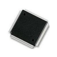
MC9S12DT256MPVE Freescale Semiconductor, MC9S12DT256MPVE Datasheet - Page 691

MC9S12DT256MPVE
Manufacturer Part Number
MC9S12DT256MPVE
Description
IC MCU 256K FLASH 25MHZ 112-LQFP
Manufacturer
Freescale Semiconductor
Series
HCS12r
Datasheet
1.S912XDG128F2MAL.pdf
(1348 pages)
Specifications of MC9S12DT256MPVE
Core Processor
HCS12
Core Size
16-Bit
Speed
25MHz
Connectivity
CAN, I²C, SCI, SPI
Peripherals
PWM, WDT
Number Of I /o
91
Program Memory Size
256KB (256K x 8)
Program Memory Type
FLASH
Eeprom Size
4K x 8
Ram Size
12K x 8
Voltage - Supply (vcc/vdd)
2.35 V ~ 5.25 V
Data Converters
A/D 8x10b
Oscillator Type
Internal
Operating Temperature
-40°C ~ 125°C
Package / Case
112-LQFP
Processor Series
S12D
Core
HCS12
Data Bus Width
16 bit
Data Ram Size
12 KB
Interface Type
CAN/I2C/SCI/SPI
Maximum Clock Frequency
25 MHz
Number Of Programmable I/os
91
Number Of Timers
1
Operating Supply Voltage
5 V to 2.5 V
Maximum Operating Temperature
+ 125 C
Mounting Style
SMD/SMT
3rd Party Development Tools
EWHCS12
Development Tools By Supplier
M68KIT912DP256
Minimum Operating Temperature
- 40 C
On-chip Adc
2 (8-ch x 10-bit)
No. Of I/o's
91
Eeprom Memory Size
4KB
Ram Memory Size
12KB
Cpu Speed
25MHz
No. Of Timers
1
No. Of Pwm Channels
8
Digital Ic Case Style
LQFP
Rohs Compliant
Yes
Lead Free Status / RoHS Status
Lead free / RoHS Compliant
Available stocks
Company
Part Number
Manufacturer
Quantity
Price
Company:
Part Number:
MC9S12DT256MPVE
Manufacturer:
Freescale Semiconductor
Quantity:
10 000
- Current page: 691 of 1348
- Download datasheet (8Mb)
Chapter 19
S12X Debug (S12XDBGV2) Module
19.1
Introduction
The DBG module provides an on-chip trace buffer with flexible triggering capability to allow non-intrusive
debug of application software. The DBG module is optimized for the HCS12X 16-bit architecture and
allows debugging of both CPU and XGATE module operations.
Typically the DBG module is used in conjunction with the BDM module, whereby the user configures the
DBG module for a debugging session over the BDM interface. Once configured the DBG module is armed
and the device leaves BDM mode returning control to the user program, which is then monitored by the
DBG module. Alternatively, the DBG module can be configured over a serial interface using SWI routines.
Comparators monitor the bus activity of the CPU and XGATE modules. When a match occurs, the control
logic can trigger the state sequencer to a new state or tag an opcode. A tag hit, which occurs when the
tagged opcode reaches the execution stage of the instruction queue, can also cause a state transition.
On a transition to the final state, bus tracing is triggered and/or a breakpoint can be generated. Independent
of comparator matches, a transition to final state with associated tracing and breakpoint can be triggered
by the external TAGHI and TAGLO signals. This is done by an XGATE module S/W breakpoint request
or by writing to the TRIG control bit.
The trace buffer is visible through a 2-byte window in the register address map and can be read out using
standard 16-bit word reads. Tracing is disabled when the MCU system is secured.
19.1.1
Glossary of Terms
COF: Change Of Flow. Change in the program flow due to a conditional branch, indexed jump or interrupt.
BDM : Background Debug Mode
DUG: Device User Guide, describing the features of the device into which the DBG is integrated.
WORD: 16 bit data entity
Data Line : 64 bit data entity
XGATE : S12X family programmable Direct Memory Access Module
CPU : S12X_CPU module
Tag : Tags can be attached to XGATE or CPU opcodes as they enter the instruction pipe. If the tagged
opcode reaches the execution stage a tag hit occurs.
MC9S12XDP512 Data Sheet, Rev. 2.21
Freescale Semiconductor
693
Related parts for MC9S12DT256MPVE
Image
Part Number
Description
Manufacturer
Datasheet
Request
R
Part Number:
Description:
Manufacturer:
Freescale Semiconductor, Inc
Datasheet:
Part Number:
Description:
Manufacturer:
Freescale Semiconductor, Inc
Datasheet:
Part Number:
Description:
Manufacturer:
Freescale Semiconductor, Inc
Datasheet:
Part Number:
Description:
Manufacturer:
Freescale Semiconductor, Inc
Datasheet:
Part Number:
Description:
Manufacturer:
Freescale Semiconductor, Inc
Datasheet:
Part Number:
Description:
Manufacturer:
Freescale Semiconductor, Inc
Datasheet:
Part Number:
Description:
Manufacturer:
Freescale Semiconductor, Inc
Datasheet:
Part Number:
Description:
Manufacturer:
Freescale Semiconductor, Inc
Datasheet:
Part Number:
Description:
Manufacturer:
Freescale Semiconductor, Inc
Datasheet:
Part Number:
Description:
Manufacturer:
Freescale Semiconductor, Inc
Datasheet:
Part Number:
Description:
Manufacturer:
Freescale Semiconductor, Inc
Datasheet:
Part Number:
Description:
Manufacturer:
Freescale Semiconductor, Inc
Datasheet:
Part Number:
Description:
Manufacturer:
Freescale Semiconductor, Inc
Datasheet:
Part Number:
Description:
Manufacturer:
Freescale Semiconductor, Inc
Datasheet:
Part Number:
Description:
Manufacturer:
Freescale Semiconductor, Inc
Datasheet:


