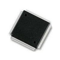
MC9S12DT256MPVE Freescale Semiconductor, MC9S12DT256MPVE Datasheet - Page 456

MC9S12DT256MPVE
Manufacturer Part Number
MC9S12DT256MPVE
Description
IC MCU 256K FLASH 25MHZ 112-LQFP
Manufacturer
Freescale Semiconductor
Series
HCS12r
Datasheet
1.S912XDG128F2MAL.pdf
(1348 pages)
Specifications of MC9S12DT256MPVE
Core Processor
HCS12
Core Size
16-Bit
Speed
25MHz
Connectivity
CAN, I²C, SCI, SPI
Peripherals
PWM, WDT
Number Of I /o
91
Program Memory Size
256KB (256K x 8)
Program Memory Type
FLASH
Eeprom Size
4K x 8
Ram Size
12K x 8
Voltage - Supply (vcc/vdd)
2.35 V ~ 5.25 V
Data Converters
A/D 8x10b
Oscillator Type
Internal
Operating Temperature
-40°C ~ 125°C
Package / Case
112-LQFP
Processor Series
S12D
Core
HCS12
Data Bus Width
16 bit
Data Ram Size
12 KB
Interface Type
CAN/I2C/SCI/SPI
Maximum Clock Frequency
25 MHz
Number Of Programmable I/os
91
Number Of Timers
1
Operating Supply Voltage
5 V to 2.5 V
Maximum Operating Temperature
+ 125 C
Mounting Style
SMD/SMT
3rd Party Development Tools
EWHCS12
Development Tools By Supplier
M68KIT912DP256
Minimum Operating Temperature
- 40 C
On-chip Adc
2 (8-ch x 10-bit)
No. Of I/o's
91
Eeprom Memory Size
4KB
Ram Memory Size
12KB
Cpu Speed
25MHz
No. Of Timers
1
No. Of Pwm Channels
8
Digital Ic Case Style
LQFP
Rohs Compliant
Yes
Lead Free Status / RoHS Status
Lead free / RoHS Compliant
Available stocks
Company
Part Number
Manufacturer
Quantity
Price
Company:
Part Number:
MC9S12DT256MPVE
Manufacturer:
Freescale Semiconductor
Quantity:
10 000
- Current page: 456 of 1348
- Download datasheet (8Mb)
Chapter 10 Freescale’s Scalable Controller Area Network (S12MSCANV3)
“MSCAN Control Register 0
stamp after the respective transmit buffer has been flagged empty.
The timer value, which is used for stamping, is taken from a free running internal CAN bit clock. A timer
overrun is not indicated by the MSCAN. The timer is reset (all bits set to 0) during initialization mode. The
CPU can only read the time stamp registers.
Read: Anytime when TXEx flag is set (see
(CANTFLG)”) and the corresponding transmit buffer is selected in CANTBSEL (see
“MSCAN Transmit Buffer Selection Register
Write: Unimplemented
10.4
10.4.1
This section provides a complete functional description of the MSCAN. It describes each of the features
and modes listed in the introduction.
456
Reset:
Reset:
W
W
Functional Description
R
R
General
TSR15
TSR7
x
x
7
7
Figure 10-37. Time Stamp Register — High Byte (TSRH)
Figure 10-38. Time Stamp Register — Low Byte (TSRL)
TSR14
TSR6
6
x
6
x
(CANCTL0)”). In case of a transmission, the CPU can only read the time
MC9S12XDP512 Data Sheet, Rev. 2.21
TSR13
TSR5
5
x
5
x
Section 10.3.2.7, “MSCAN Transmitter Flag Register
(CANTBSEL)”).
TSR12
TSR4
4
x
4
x
TSR11
TSR3
3
x
3
x
TSR10
TSR2
x
x
2
2
Freescale Semiconductor
TSR9
TSR1
Section 10.3.2.11,
x
x
1
1
TSR8
TSR0
x
x
0
0
Related parts for MC9S12DT256MPVE
Image
Part Number
Description
Manufacturer
Datasheet
Request
R
Part Number:
Description:
Manufacturer:
Freescale Semiconductor, Inc
Datasheet:
Part Number:
Description:
Manufacturer:
Freescale Semiconductor, Inc
Datasheet:
Part Number:
Description:
Manufacturer:
Freescale Semiconductor, Inc
Datasheet:
Part Number:
Description:
Manufacturer:
Freescale Semiconductor, Inc
Datasheet:
Part Number:
Description:
Manufacturer:
Freescale Semiconductor, Inc
Datasheet:
Part Number:
Description:
Manufacturer:
Freescale Semiconductor, Inc
Datasheet:
Part Number:
Description:
Manufacturer:
Freescale Semiconductor, Inc
Datasheet:
Part Number:
Description:
Manufacturer:
Freescale Semiconductor, Inc
Datasheet:
Part Number:
Description:
Manufacturer:
Freescale Semiconductor, Inc
Datasheet:
Part Number:
Description:
Manufacturer:
Freescale Semiconductor, Inc
Datasheet:
Part Number:
Description:
Manufacturer:
Freescale Semiconductor, Inc
Datasheet:
Part Number:
Description:
Manufacturer:
Freescale Semiconductor, Inc
Datasheet:
Part Number:
Description:
Manufacturer:
Freescale Semiconductor, Inc
Datasheet:
Part Number:
Description:
Manufacturer:
Freescale Semiconductor, Inc
Datasheet:
Part Number:
Description:
Manufacturer:
Freescale Semiconductor, Inc
Datasheet:


