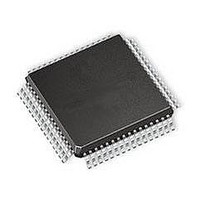
L6460 STMicroelectronics, L6460 Datasheet - Page 13

L6460
Manufacturer Part Number
L6460
Description
MOSFET & Power Driver ICs SPI Config Stepper DC Multi Motor DRV
Manufacturer
STMicroelectronics
Type
Full-Bridge Driverr
Datasheet
1.L6460.pdf
(139 pages)
Specifications of L6460
Product
Half-Bridge Drivers
Rise Time
0.4 us
Fall Time
0.4 us
Supply Voltage (max)
38 V
Supply Voltage (min)
13 V
Supply Current
11 mA
Mounting Style
SMD/SMT
Minimum Operating Temperature
- 40 C
Number Of Drivers
4
Output Current
10 mA
Output Voltage
30 V
Package / Case
TQFP-64
Lead Free Status / RoHS Status
Lead free / RoHS Compliant
Available stocks
Company
Part Number
Manufacturer
Quantity
Price
Company:
Part Number:
L6460
Manufacturer:
MICROCHIP
Quantity:
998
L6460
Table 2.
1. These pins must be connected all together to a unique PCB ground.
2. Bridges1 and 2 have 2 ground pads: one is bonded to the relative ground pin (GND1 or GND2) and the
3. The analog ground is connected to exposed pad E-Pad.
4. The pin must be tied to ground if bridge is not used as a stepper motor.
E_Pad
Pin #
35
36
37
38
39
40
41
42
43
44
45
46
47
48
49
50
51
52
53
54
55
56
57
58
59
60
61
62
63
64
other is connected to exposed pad (E_Pad) ground ring. This makes the bond wires testing possible by
forcing a current between E-Pad and GND1 or GND2 pins and using the other pin as sense pin to measure
the resistance of E-Pad bonding. (N.B: grounds of two bridges are internally connected together).
V
DC4_SENSE Bridge 4 sense output
DC3_SENSE Bridge 3 sense output
DC3_SENSE Bridge 3 sense output
DC4_MINUS Bridge 4 phase “minus” output
DC3_MINUS Bridge 3 phase “minus” output
V
DC3_PLUS
SWDRV_GATE
GND_PAD
Pin name
V
DC1_plus
V
SWDRV_SW
nRESET
GPIO12
GPIO13
GPIO14
GPIO11
GPIO10
GPIO9
GPIO5
V
GPIO7
GPIO_SPI
GPIO6
V
SupplyInt
V
CPH
Pins configuration (continued)
N.C.
N.C.
N.C.
V
CPL
Supply
Supply
Pump
3v3
General purpose I/O
General purpose I/O
General purpose I/O
Not connected
Not connected
General purpose I/O
General purpose I/O
General purpose I/O
General purpose I/O
Not connected
Bridge 3 phase “plus” output
Main voltage supply
Open drain system reset pin
Internal 3.3 volt regulator
Internal voltage supply
General purpose I/O
Low voltage pins power supply
General purpose I/O
Switching regulator controller source input
Switching driver gate drive pin
Charge pump voltage
Charge pump high switch pin
Charge pump low switch pin
Main voltage supply
Bridge 1 phase “plus” output
(1)(2)(3)
Doc ID 17713 Rev 1
Description
(4)
(4)
(4)
Analog In/Out - CMOS bi-dir
Analog In/Out - CMOS bi-dir
Analog In/Out - CMOS bi-dir
Analog In/Out - CMOS bi-dir
Analog In/Out - CMOS bi-dir
Analog In/Out - CMOS bi-dir
Analog In/Out - CMOS bi-dir
Analog In/Out - CMOS bi-dir
Analog In/Out - CMOS bi-dir
CMOS Input/output
Power Input/output
Power Input/output
Power Input/output
Power Input/output
General description
Analog output
Power Input
Power input
Power input
Power input
Power input
Output
Output
Output
Output
Output
Output
Output
Type
13/139


