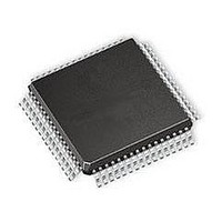
L6460 STMicroelectronics, L6460 Datasheet - Page 28

L6460
Manufacturer Part Number
L6460
Description
MOSFET & Power Driver ICs SPI Config Stepper DC Multi Motor DRV
Manufacturer
STMicroelectronics
Type
Full-Bridge Driverr
Datasheet
1.L6460.pdf
(139 pages)
Specifications of L6460
Product
Half-Bridge Drivers
Rise Time
0.4 us
Fall Time
0.4 us
Supply Voltage (max)
38 V
Supply Voltage (min)
13 V
Supply Current
11 mA
Mounting Style
SMD/SMT
Minimum Operating Temperature
- 40 C
Number Of Drivers
4
Output Current
10 mA
Output Voltage
30 V
Package / Case
TQFP-64
Lead Free Status / RoHS Status
Lead free / RoHS Compliant
Available stocks
Company
Part Number
Manufacturer
Quantity
Price
Company:
Part Number:
L6460
Manufacturer:
MICROCHIP
Quantity:
998
Electrical specifications
Table 5.
1. This value is useful to define the voltage rating for external capacitor to be connected from V
2. This typical value is only intended to give an estimation of the current consumption when L6460 is configured in simple
3. Measured between 10% and 90% of output voltage transition.
4. Measured from a fault detection to 50% of output voltage transition.
5. Current is defined to be positive when flowing into the pin.
6. Load regulation is calculated at a fixed junction temperature using short load pulses covering all the load current range. This
7. Undervoltage rising and falling thresholds are intended as a percentage of feedback pin voltage (V
8. Default state.
9. The regulated voltage can be calculated using the formula: V
28/139
SPI interface
t
regulators mode (see following
typical value allows a raw choose of the external resistor but the definitive choose must be done according to the
recommendations on
is to avoid change on output voltage due to heating effect.
Parameter
t
MISO_disable
t
t
t
t
MOSI_setup
t
t
t
t
MISO_valid
SCLK_high
t
MOSI_hold
t
SCLK_rise
nSS_setup
SCLK_low
t
MISO_rise
SCLK_fall
MISO_fall
nSS_hold
nSS_min
C
t
t
DELAY
V
V
SCLK
V
V
LOAD
I
V
HYS
AD
OH
OL
IH
IL
Electrical characteristics (continued)
(40)
A/D path absorbed current
Delay from serial write to pin
low
High level input voltage
Low level input voltage
Input voltage hysteresis
High level output voltage
Low level output voltage
SCLK period
SCLK rise time
SCLK fall time
SCLK high time
SCLK low time
nSS setup time
nSS hold time
nSS high minimum time
MOSI setup time
MOSI hold time
MISO rise time
MISO fall time
MISO valid from clock low
MISO disable time
MOSI maximum load
Chapter
Description
4.1).
Chapter
8.6.4) at the end of the start up sequence and with no load on regulators. This
Doc ID 17713 Rev 1
ADChannelX[4:0]
=10001 and
bit EnDacScale=0
C
(46)
(46)
(46)
I
I
C
C
OUT
OUT
LOAD
LOAD
LOAD
= -10mA,
= 10mA,
SWmain_OUT =
Test condition
=50pF
=50pF
=50 pF
(48)
(47)
(48)
(45)
(47)
V
FBREF
*(R
a
+R
0.15
2.75
62.5
Min
1.6
b
20
20
10
10
30
10
10
-1
)/R
0
0
Supply
b
.
LINmain_FB
to V
0.22
Typ
SupplyInt
).
Max
500
200
0.8
0.4
.
15
15
1
2
2
9
9
L6460
Unit
µA
pF
ns
ns
ns
ns
ns
ns
ns
ns
ns
ns
ns
ns
ns
ns
ns
V
V
V
V
V


