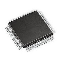
L6460 STMicroelectronics, L6460 Datasheet - Page 29

L6460
Manufacturer Part Number
L6460
Description
MOSFET & Power Driver ICs SPI Config Stepper DC Multi Motor DRV
Manufacturer
STMicroelectronics
Type
Full-Bridge Driverr
Datasheet
1.L6460.pdf
(139 pages)
Specifications of L6460
Product
Half-Bridge Drivers
Rise Time
0.4 us
Fall Time
0.4 us
Supply Voltage (max)
38 V
Supply Voltage (min)
13 V
Supply Current
11 mA
Mounting Style
SMD/SMT
Minimum Operating Temperature
- 40 C
Number Of Drivers
4
Output Current
10 mA
Output Voltage
30 V
Package / Case
TQFP-64
Lead Free Status / RoHS Status
Lead free / RoHS Compliant
Available stocks
Company
Part Number
Manufacturer
Quantity
Price
Company:
Part Number:
L6460
Manufacturer:
MICROCHIP
Quantity:
998
L6460
10. Undervoltage rising and falling thresholds are intended as a percentage of feedback pin voltage (V
11. This condition is intended to simulate an extra current on output.
12. This condition is intended to simulate a short circuit on output.
13. Rise and fall time are measured between 10% and 90% V
14. Undervoltage rising and falling thresholds are intended as a percentage of feedback pin voltage (V
15. The current protection values must be intended as a protection for the chip and not as a continuous current limitation. The
16. In this cell X stands for 1 or 2, Y stands for A or B
17. In this cell X stands for 3 or 4, Y stands for A or B
18. The current protection thresholds for Bridge 3 and 4 are not selectable so only the max current value
19. Overcurrent Off time can be configured using SPI.
20. Rise and fall time are measured between 10% and 90% of DC output voltage. With device in full bridge configuration
21. Default state for Aux1
22. Default state for Aux2
23. The regulated voltage can be calculated using the formula: V
24. Undervoltage rising and falling thresholds are intended as a percentage of feedback pin voltage (GPIO1 and/or GPIO2)
25. Rise and fall time is measured between 10% and 90% of output voltage.
26. The external components connected to the pin must be chosen to avoid that the voltage exceeds this operative range.
27. The regulated voltage can be calculated using the formula: V
28. Undervoltage rising and falling thresholds are intended as a percentage of feedback pin voltage (V
29. The definition of LSB for this table is LSB=IMRmax/(2
30. Integral Non Linearity error (INL) is defined as the maximum distance between any point of the ADC characteristic and the
31. The ADC ensures monotonic characteristic and no missing codes.
32. Differential nonlinearity error (DNL) is defined as the difference between an actual step width and the ideal width value of 1
33. Offset error (OE) is the deviation of the first code transition (000...000 to 000...001) from the ideal (i.e. GND + 0.5 LSB).
34. Gain error (GE) is the deviation of the last code transition (111...110 to 111...111) from the ideal (V3v3 - 0.5 LSB), after
35. Please note that the result of the conversion will always be a 9-bit word: to speed up the conversion, the resolution is
36. Actual input capacitance depends on the pin that must be converted.
37. The definition of LSB for this table is LSB=IMRmax/(2
38. All parameters are guaranteed in the range between V
39. Measured from DacValue[5:0] change in SPI interface.
40. V
41. In this section reports the operational amplifier parameters that change when used as comparator.
42. ΔVi is the differential voltage applied to input pins across the common voltage V
43. Measured between 50% of input and output signal.
44. Time measured from change in SPI interface to 50% of external pin transition.
45. Measured between nSS rising edge and 50% of V
46. Specification applies to nSS, SCLK and MOSI pins.
47. Current is considered to be positive when flowing towards the IC
48. These times are measured at the pin output between specified V
protection is performed by switching off the output bridge when current reaches values higher than the I
protection could be guaranteed for values in the middle range between I
(MtrXSideYILimSel[1:0]= 11) is available.
(resistive load between outputs).
“best straight line” approximating the ADC transfer curve.
LSB.
adjusting for offset error.
reduced when the ADC is used in the 8- bit resolution mode.
GPIO_SPI
= 3.3 V unless otherwise specified
Doc ID 17713 Rev 1
out
.
7.5
9
-1).
OL
-1).
and V
SWmain
AUX_SW
AUX3_SW
R Max
OH
output voltage.
and V
.
= V
= V
MAX
FBREF
FBREF
OL
.
and I
*(R
CM
*(R
OC
a
.
+R
a
+R
b
)/R
b
)/R
b
.
b
.
Electrical specifications
SW_main_FB
SWDRV_FB
REF_FB
OC
).
max. No
).
).
29/139


