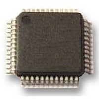
UPD78F0413GA-GAM-AX NEC, UPD78F0413GA-GAM-AX Datasheet - Page 306

UPD78F0413GA-GAM-AX
Manufacturer Part Number
UPD78F0413GA-GAM-AX
Description
8BIT UC, 32K FLASH, 1KB RAM, LCD
Manufacturer
NEC
Datasheet
1.UPD78F0413GA-GAM-AX.pdf
(562 pages)
Specifications of UPD78F0413GA-GAM-AX
Controller Family/series
UPD78F
No. Of I/o's
30
Ram Memory Size
1024Byte
Cpu Speed
10MHz
No. Of Timers
8
No. Of Pwm
RoHS Compliant
Core Size
8bit
Program Memory Size
32KB
Oscillator Type
External, Internal
Available stocks
Company
Part Number
Manufacturer
Quantity
Price
Company:
Part Number:
UPD78F0413GA-GAM-AX
Manufacturer:
ADI
Quantity:
882
Company:
Part Number:
UPD78F0413GA-GAM-AX
Manufacturer:
Renesas Electronics America
Quantity:
10 000
- Current page: 306 of 562
- Download datasheet (4Mb)
306
The setting methods are described below.
<Change the channel>
<Complete A/D conversion>
<1> Set bit 0 (ADCE) of the A/D converter mode register (ADM) to 1.
<2> Set the channel to be used in the analog input mode by using bits 2 to 0 (ADPC02 to ADPC00) of the
<3> Select conversion time by using bits 6 to 1 (FR3 to FR0, LV1, and LV0) of ADM.
<4> Select a channel to be used by using bits 2 to 0 (ADS2 to ADS0) of the analog input channel
<5> Set bit 7 (ADCS) of ADM to 1 to start A/D conversion.
<6> When one A/D conversion has been completed, an interrupt request signal (INTAD) is generated.
<7> Transfer the A/D conversion data to the A/D conversion result register (ADCR, ADCRH).
<8> Change the channel using bits 2 to 0 (ADS2 to ADS0) of ADS to start A/D conversion.
<9> When one A/D conversion has been completed, an interrupt request signal (INTAD) is generated.
<10> Transfer the A/D conversion data to the A/D conversion result register (ADCR, ADCRH).
<11> Clear ADCS to 0.
<12> Clear ADCE to 0.
Cautions 1. Make sure the period of <1> to <5> is 1 s or more.
CHAPTER 12 10-BIT SUCCESSIVE APPROXIMATION TYPE A/D CONVERTER ( PD78F041x only)
A/D port configuration register 0 (ADPC0) and bits 5 to 0 (PM25 to PM20) of port mode register 2 (PM2).
specification register (ADS).
2. <1> may be done between <2> and <4>.
3. <1> can be omitted. However, ignore data of the first conversion after <5> in this case.
4. The period from <6> to <9> differs from the conversion time set using bits 6 to 1 (FR3 to
FR0, LV1, LV0) of ADM. The period from <8> to <9> is the conversion time set using FR3
to FR0, LV1, and LV0.
User’s Manual U18698EJ1V0UD
Related parts for UPD78F0413GA-GAM-AX
Image
Part Number
Description
Manufacturer
Datasheet
Request
R

Part Number:
Description:
16/8 bit single-chip microcomputer
Manufacturer:
NEC
Datasheet:

Part Number:
Description:
Dual audio power amp circuit
Manufacturer:
NEC
Datasheet:

Part Number:
Description:
Dual comparator
Manufacturer:
NEC
Datasheet:

Part Number:
Description:
MOS type composite field effect transistor
Manufacturer:
NEC
Datasheet:

Part Number:
Description:
50 V/100 mA FET array incorporating 2 N-ch MOSFETs
Manufacturer:
NEC
Datasheet:

Part Number:
Description:
6-pin small MM high-frequency double transistor
Manufacturer:
NEC
Datasheet:

Part Number:
Description:
6-pin small MM high-frequency double transistor
Manufacturer:
NEC
Datasheet:

Part Number:
Description:
6-pin small MM high-frequency double transistor
Manufacturer:
NEC
Datasheet:

Part Number:
Description:
6-pin small MM high-frequency double transistor
Manufacturer:
NEC
Datasheet:

Part Number:
Description:
Twin transistors equipped with different model chips(6P small MM)
Manufacturer:
NEC
Datasheet:

Part Number:
Description:
Bipolar analog integrated circuit
Manufacturer:
NEC
Datasheet:


