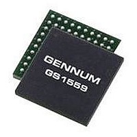
GS1559CBE2 GENNUM, GS1559CBE2 Datasheet - Page 13

GS1559CBE2
Manufacturer Part Number
GS1559CBE2
Description
IC, DES, 48.5MHZ 20BIT 1.485GBPS BGA-100
Manufacturer
GENNUM
Datasheet
1.GS1559CBE2.pdf
(73 pages)
Specifications of GS1559CBE2
Supply Voltage Range
1.71V To 1.89V, 3.13V To 3.47V
Operating Temperature Range
0°C To +70°C
Digital Ic Case Style
BGA
No. Of Pins
100
Termination Type
SMD
Control Interface
Serial
Lead Free Status / RoHS Status
Lead free / RoHS Compliant
Table 1-1: Pin Descriptions (Continued)
Number
Pin
G8
H2
H4
H5
H6
H7
DATA_ERROR
SDOUT_TDO
SCLK_TCK
FIFO_LD
CS_TMS
Name
TERM2
Synchronous
Synchronous
Synchronous
Synchronous
Synchronous
SCLK_TCK
SCLK_TCK
with PCLK
with PCLK
30572 - 7
Timing
Analog
with
Non
with
May 2007
Output
Output
Output
Type
Input
Input
Input
Description
CONTROL SIGNAL OUTPUT
Signal levels are LVCMOS/LVTTL compatible.
Used as a control signal for external FIFO(s).
Normally HIGH but will go LOW for one PCLK period at SAV.
Termination for serial digital input 2. AC couple to EQ_GND.
CONTROL SIGNAL INPUT
Signal levels are LVCMOS/LVTTL compatible.
Chip Select / Test Mode Select
Host Mode (JTAG/HOST = LOW)
CS_TMS operates as the host interface chip select, CS, and is active
LOW.
JTAG Test Mode (JTAG/HOST = HIGH)
CS_TMS operates as the JTAG test mode select, TMS, and is active
HIGH.
NOTE: If the host interface is not being used, tie this pin HIGH.
CONTROL SIGNAL INPUT
Signal levels are LVCMOS/LVTTL compatible.
Serial Data Clock / Test Clock.
Host Mode (JTAG/HOST = LOW)
SCLK_TCK operates as the host interface burst clock, SCLK. Command
and data read/write words are clocked into the device synchronously with
this clock.
JTAG Test Mode (JTAG/HOST = HIGH)
SCLK_TCK operates as the JTAG test clock, TCK.
NOTE: If the host interface is not being used, tie this pin HIGH.
CONTROL SIGNAL OUTPUT
Signal levels are LVCMOS/LVTTL compatible.
Serial Data Output / Test Data Output
Host Mode (JTAG/HOST = LOW)
SDOUT_TDO operates as the host interface serial output, SDOUT, used
to read status and configuration information from the internal registers of
the device.
JTAG Test Mode (JTAG/HOST = HIGH)
SDOUT_TDO operates as the JTAG test data output, TDO.
STATUS SIGNAL OUTPUT
Signal levels are LVCMOS/LVTTL compatible.
The DATA_ERROR signal will be LOW when an error within the received
data stream has been detected by the device. This pin is a logical 'OR'ing
of all detectable errors listed in the internal ERROR_STATUS register.
Once an error is detected, DATA_ERROR will remain LOW until the start
of the next video frame / field, or until the ERROR_STATUS register is
read via the host interface.
The DATA_ERROR signal will be HIGH when the received data stream
has been detected without error.
NOTE: It is possible to program which error conditions are monitored by
the device by setting appropriate bits of the ERROR_MASK register HIGH.
All error conditions are detected by default.
GS1559 Data Sheet
13 of 73


