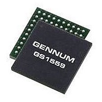
GS1559CBE2 GENNUM, GS1559CBE2 Datasheet - Page 43

GS1559CBE2
Manufacturer Part Number
GS1559CBE2
Description
IC, DES, 48.5MHZ 20BIT 1.485GBPS BGA-100
Manufacturer
GENNUM
Datasheet
1.GS1559CBE2.pdf
(73 pages)
Specifications of GS1559CBE2
Supply Voltage Range
1.71V To 1.89V, 3.13V To 3.47V
Operating Temperature Range
0°C To +70°C
Digital Ic Case Style
BGA
No. Of Pins
100
Termination Type
SMD
Control Interface
Serial
Lead Free Status / RoHS Status
Lead free / RoHS Compliant
- Current page: 43 of 73
- Download datasheet (2Mb)
4.10.2 Ancillary Data Detection and Indication
Y/Cr/Cb DATA OUT
MULTIPLEXED
FIFO_LD
PCLK
Y/Cr/Cb DATA OUT
CHROMA DATA OUT
LUMA DATA OUT
MULTIPLEXED
3FF
CHROMA DATA OUT
FIFO_LD
FIFO_LD
PCLK
LUMA DATA OUT
PCLK
Figure 4-5: FIFO_LD Pulse Timing
The GS1559 will detect all types of ancillary data in either the vertical or horizontal
blanking spaces and indicate via the status signal output pins YANC and CANC the
position of ancillary data in the output data stream. These status signal outputs are
synchronous with PCLK and can be used as clock enables to external logic, or as
write enables to an external FIFO or other memory device.
When operating in HD mode, (SD/HD = LOW), the YANC signal will be HIGH
whenever ancillary data is detected in the luma data stream, and the CANC signal
will be HIGH whenever ancillary data is detected in the chroma data stream.
30572 - 7
FIFO_LD
3FF
PCLK
May 2007
3FF
FIFO LOAD PULSE - SD 10BIT OUTPUT MODE
FIFO LOAD PULSE - SD 20BIT OUTPUT MODE
FIFO LOAD PULSE - HD 20BIT OUTPUT MODE
FIFO LOAD PULSE - HD 10BIT OUTPUT MODE
3FF
3FF
000
000
3FF
000
000
000
000
(SAV)
000
XYZ
000
000
000
000
(SAV)
XYZ
(SAV)
(SAV)
XYZ
XYZ
000
GS1559 Data Sheet
(SAV)
XYZ
(SAV)
XYZ
43 of 73
Related parts for GS1559CBE2
Image
Part Number
Description
Manufacturer
Datasheet
Request
R

Part Number:
Description:
GS1559 HD-LINX-TM II Multi-Rate Deserializer with Loop-Through Cable Driver
Manufacturer:
Gennum Corp.
Datasheet:

Part Number:
Description:
HD-LINX II Multi-Rate Deserializer with Loop-Through Cable Driver
Manufacturer:
Gennum Corp.
Datasheet:

Part Number:
Description:
Wideband, monolithic 1x1 video crosspoint switch
Manufacturer:
Gennum Corporation
Datasheet:

Part Number:
Description:
Wideband, Monolithic 4x1 Video Multiplexer
Manufacturer:
Gennum Corporation
Datasheet:

Part Number:
Description:
Monolithic 4x1 Video Multiplexer
Manufacturer:
Gennum Corporation
Datasheet:

Part Number:
Description:
Low Distortion AGC Amplifier
Manufacturer:
Gennum Corporation
Datasheet:


