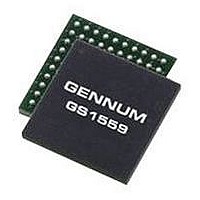
GS1559CBE2 GENNUM, GS1559CBE2 Datasheet - Page 15

GS1559CBE2
Manufacturer Part Number
GS1559CBE2
Description
IC, DES, 48.5MHZ 20BIT 1.485GBPS BGA-100
Manufacturer
GENNUM
Datasheet
1.GS1559CBE2.pdf
(73 pages)
Specifications of GS1559CBE2
Supply Voltage Range
1.71V To 1.89V, 3.13V To 3.47V
Operating Temperature Range
0°C To +70°C
Digital Ic Case Style
BGA
No. Of Pins
100
Termination Type
SMD
Control Interface
Serial
Lead Free Status / RoHS Status
Lead free / RoHS Compliant
- Current page: 15 of 73
- Download datasheet (2Mb)
Table 1-1: Pin Descriptions (Continued)
Number
K3, K4
Pin
K2
K5
K6
K7
JTAG/HOST
SDO, SDO
CD_GND
CD_VDD
Name
F
Synchronous
Synchronous
with PCLK
30572 - 7
Timing
Analog
Non
–
–
May 2007
Output
Output
Power
Power
Type
Input
Description
Power supply connection for the serial digital cable driver. Connect to
+1.8V DC analog.
Serial digital loop-through output signal operating at 1.485Gb/s,
1.485/1.001Gb/s, or 270Mb/s.
The slew rate of these outputs is automatically controlled to meet SMPTE
292M and 259M requirements according to the setting of the SD/HD pin.
Ground connection for the serial digital cable driver. Connect to analog
GND.
CONTROL SIGNAL INPUT
Signal levels are LVCMOS/LVTTL compatible.
Used to select JTAG Test Mode or Host Interface Mode.
When set HIGH, CS_TMS, SDOUT_TDO, SDI_TDI and SCLK_TCK are
configured for JTAG boundary scan testing.
When set LOW, CS_TMS, SDOUT_TDO, SDI_TDI and SCLK_TCK are
configured as GSPI pins for normal host interface operation.
STATUS SIGNAL OUTPUT
Signal levels are LVCMOS/LVTTL compatible.
Used to indicate the ODD / EVEN field of the video signal.
The F signal will be HIGH for the entire period of field 2 as indicated by the
F bit in the received TRS signals.
The F signal will be LOW for all lines in field 1 and for all lines in
progressive scan systems.
GS1559 Data Sheet
15 of 73
Related parts for GS1559CBE2
Image
Part Number
Description
Manufacturer
Datasheet
Request
R

Part Number:
Description:
GS1559 HD-LINX-TM II Multi-Rate Deserializer with Loop-Through Cable Driver
Manufacturer:
Gennum Corp.
Datasheet:

Part Number:
Description:
HD-LINX II Multi-Rate Deserializer with Loop-Through Cable Driver
Manufacturer:
Gennum Corp.
Datasheet:

Part Number:
Description:
Wideband, monolithic 1x1 video crosspoint switch
Manufacturer:
Gennum Corporation
Datasheet:

Part Number:
Description:
Wideband, Monolithic 4x1 Video Multiplexer
Manufacturer:
Gennum Corporation
Datasheet:

Part Number:
Description:
Monolithic 4x1 Video Multiplexer
Manufacturer:
Gennum Corporation
Datasheet:

Part Number:
Description:
Low Distortion AGC Amplifier
Manufacturer:
Gennum Corporation
Datasheet:


