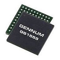
GS1559CBE2 GENNUM, GS1559CBE2 Datasheet - Page 29

GS1559CBE2
Manufacturer Part Number
GS1559CBE2
Description
IC, DES, 48.5MHZ 20BIT 1.485GBPS BGA-100
Manufacturer
GENNUM
Datasheet
1.GS1559CBE2.pdf
(73 pages)
Specifications of GS1559CBE2
Supply Voltage Range
1.71V To 1.89V, 3.13V To 3.47V
Operating Temperature Range
0°C To +70°C
Digital Ic Case Style
BGA
No. Of Pins
100
Termination Type
SMD
Control Interface
Serial
Lead Free Status / RoHS Status
Lead free / RoHS Compliant
- Current page: 29 of 73
- Download datasheet (2Mb)
4.4.1 Output Swing
4.4.2 Reclocker Bypass Control
Nominally, the voltage swing of the serial digital loop-through output is 800mV
single-ended into a 75Ω load. This is set externally by connecting the RSET pin to
CD_VDD through 281Ω.
The loop-through output swing may be decreased by increasing the value of the
RSET resistor. The relationship is approximated by the curve shown in
Alternatively, the serial digital output can drive 800mVp-p into a 50Ω load. Since
the output swing is reduced by a factor of approximately one third when the smaller
load is used, the RSET resistor must be 187Ω to obtain 800mVp-p.
Figure 4-1: Serial Digital Loop-Through Output Swing
The serial digital loop-through output may be either a buffered version of the serial
digital input signal, or a reclocked version of that signal.
When operating in slave mode, the application layer may choose the reclocked
output by setting RC_BYP to logic HIGH. If RC_BYP is set LOW, the data stream
will bypass the internal reclocker and the serial digital output will be a buffered
version of the input.
When operating in master mode, the device will assert the RC_BYP pin HIGH only
when it has successfully locked to a SMPTE or DVB-ASI input data stream, (see
Lock Detect on page
a reclocked version of the input.
30572 - 7
1000
900
800
700
600
500
400
300
250
May 2007
300
350
400
31). In this case, the serial digital loop-through output will be
450
RSET(Ω)
500
550
600
650
700
750
GS1559 Data Sheet
Figure
29 of 73
4-1.
p-p
Related parts for GS1559CBE2
Image
Part Number
Description
Manufacturer
Datasheet
Request
R

Part Number:
Description:
GS1559 HD-LINX-TM II Multi-Rate Deserializer with Loop-Through Cable Driver
Manufacturer:
Gennum Corp.
Datasheet:

Part Number:
Description:
HD-LINX II Multi-Rate Deserializer with Loop-Through Cable Driver
Manufacturer:
Gennum Corp.
Datasheet:

Part Number:
Description:
Wideband, monolithic 1x1 video crosspoint switch
Manufacturer:
Gennum Corporation
Datasheet:

Part Number:
Description:
Wideband, Monolithic 4x1 Video Multiplexer
Manufacturer:
Gennum Corporation
Datasheet:

Part Number:
Description:
Monolithic 4x1 Video Multiplexer
Manufacturer:
Gennum Corporation
Datasheet:

Part Number:
Description:
Low Distortion AGC Amplifier
Manufacturer:
Gennum Corporation
Datasheet:


