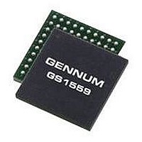
GS1559CBE2 GENNUM, GS1559CBE2 Datasheet - Page 28

GS1559CBE2
Manufacturer Part Number
GS1559CBE2
Description
IC, DES, 48.5MHZ 20BIT 1.485GBPS BGA-100
Manufacturer
GENNUM
Datasheet
1.GS1559CBE2.pdf
(73 pages)
Specifications of GS1559CBE2
Supply Voltage Range
1.71V To 1.89V, 3.13V To 3.47V
Operating Temperature Range
0°C To +70°C
Digital Ic Case Style
BGA
No. Of Pins
100
Termination Type
SMD
Control Interface
Serial
Lead Free Status / RoHS Status
Lead free / RoHS Compliant
4.3.1 External VCO
4.3.2 Loop Bandwidth
4.4 Serial Digital Loop-Through Output
The GS1559 requires the external GO1555/GO1525* Voltage Controlled Oscillator
as part of the reclocker's phase-locked loop. This external VCO implementation
was chosen to ensure high quality reclocking.
Power for the external VCO is generated entirely by the GS1559 from an integrated
voltage regulator. The internal regulator uses +3.3V DC supplied via the CP_VDD
/ CP_GND pins to provide +2.5V DC on the VCO_VCC / VCO_GND pins.
The control voltage to the VCO is output from the GS1559 on the LF pin and
requires 4.7kΩ pull-up and pull-down resistors to ensure correct operation.
The GO1555/GO1525* produces a 1.485GHz reference signal for the reclocker,
input on the VCO pin of the GS1559. Both LF and VCO signals should be
referenced to the supplied VCO_GND as shown in the recommended application
circuit of
*For new designs use GO1555
The loop bandwidth of the integrated reclocker is nominally 1.4MHz, but may be
increased or decreased via the LB_CONT pin. It is recommended that this pin be
connected to VCO_GND through 39.2kΩ to maximize the input jitter tolerance of
the device.
The GS1559 contains an integrated current mode differential serial digital cable
driver with automatic slew rate control. When enabled, this serial digital output
provides an active loop-through of the input signal.
The integrated cable driver uses a separate power supply of +1.8V DC supplied via
the CD_VDD and CD_GND pins.
To enable the loop-through output, SDO_EN/DIS must be set HIGH by the
application layer. Setting the SDO_EN/DIS signal LOW will cause the SDO and
SDO output pins to become high impedance, resulting in reduced device power
consumption.
When not using the serial digital output from the GS1559, the SDO and SDO pins
should be left unconnected (floating). In addition, the SDO_EN pin should be set
LOW and the RSET pin may be AC terminated to analog ground through a 10nF
capacitor.
Gennum recommends using the GS1528A SDI Dual Slew-Rate Cable Driver to
meet SMPTE specifications.
30572 - 7
Typical Application Circuit (Part A) on page
May 2007
68.
GS1559 Data Sheet
28 of 73


