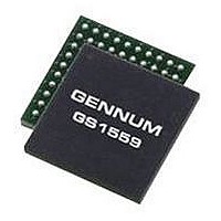
GS1559CBE2 GENNUM, GS1559CBE2 Datasheet - Page 73

GS1559CBE2
Manufacturer Part Number
GS1559CBE2
Description
IC, DES, 48.5MHZ 20BIT 1.485GBPS BGA-100
Manufacturer
GENNUM
Datasheet
1.GS1559CBE2.pdf
(73 pages)
Specifications of GS1559CBE2
Supply Voltage Range
1.71V To 1.89V, 3.13V To 3.47V
Operating Temperature Range
0°C To +70°C
Digital Ic Case Style
BGA
No. Of Pins
100
Termination Type
SMD
Control Interface
Serial
Lead Free Status / RoHS Status
Lead free / RoHS Compliant
8. Revision History
Version
2
3
4
5
6
7
ECR
136173
136980
137523
140420
143592
145031
PCN
–
–
–
39452
42774
–
GENNUM CORPORATION
Mailing Address: P.O. Box 489, Stn. A, Burlington, Ontario, Canada L7R 3Y3
Shipping Address: 970 Fraser Drive, Burlington, Ontario, Canada L7L 5P5
Tel. +1 (905) 632-2996 Fax. +1 (905) 632-5946
GENNUM JAPAN CORPORATION
Shinjuku Green Tower Building 27F, 6-14-1, Nishi Shinjuku, Shinjuku-ku, Tokyo, 160-0023 Japan
Tel. +81 (03) 3349-5501, Fax. +81 (03) 3349-5505
GENNUM UK LIMITED
25 Long Garden Walk, Farnham, Surrey, England GU9 7HX
Tel. +44 (0)1252 747 000 Fax +44 (0)1252 726 523
Gennum Corporation assumes no liability for any errors or omissions in this document, or for the use of the
circuits or devices described herein. The sale of the circuit or device described herein does not imply any
patent license, and Gennum makes no representation that the circuit or device is free from patent
infringement.
GENNUM and the G logo are registered trademarks of Gennum Corporation.
© Copyright 2004 Gennum Corporation. All rights reserved. Printed in Canada.
30572 - 7
Date
April 2005
June 2005
July 2005
May 2006
January 2007
May 2007
DOCUMENT IDENTIFICATION
DATA SHEET
The product is in production. Gennum reserves the right to make
changes at any time to improve reliability, function or design, in order to
provide the best product possible.
CAUTION
ELECTROSTATIC SENSITIVE DEVICES
DO NOT OPEN PACKAGES OR HANDLE
EXCEPT AT A STATIC-FREE WORKSTATION
May 2007
Changes and / or Modifications
Corrected GSPI Input Data Hold Time in AC Electrical Characteristics
table. Updated SCLK to show as a burst clock. Removed references to
part being “Green”. Clarified setting of VD_STD[4:0], INT_PROG and
STD_LOCK bits following a reset and/or removal of input. Updated
Typical Application cirucit A. Corrected minor typing errors.
Restored missing overlines. Corrected missing TERM pin in Serial Digital
Input connection diagram. Changed note on ESD protection. Corrected
Section
Data Sheet.
Corrected ground symbol in
page
Corrected minor typing errors in Functional Block Diagram. Modified
video format numbers for system 1125 on
for Digital
Added RoHS compliance statement to
Recommended GO1555 VCO for new designs.
Updated description of H2 from PDBUFF_GND to EQ_GND in
Pin
Application Circuit (Part
Descriptions. Changed GND_EQ to EQ_GND in
69.
4.2.3. Added note on unused output to
Systems.
73
B).
Typical Application Circuit (Part B) on
Section 7.2 Packaging
GS1559 Data Sheet
Table 4-4: Switch Line Position
Section
5.2 Typical
4.4. Converted to
Data.
Table 1-1:
73 of 73


