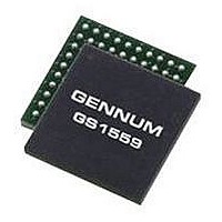
GS1559CBE2 GENNUM, GS1559CBE2 Datasheet - Page 39

GS1559CBE2
Manufacturer Part Number
GS1559CBE2
Description
IC, DES, 48.5MHZ 20BIT 1.485GBPS BGA-100
Manufacturer
GENNUM
Datasheet
1.GS1559CBE2.pdf
(73 pages)
Specifications of GS1559CBE2
Supply Voltage Range
1.71V To 1.89V, 3.13V To 3.47V
Operating Temperature Range
0°C To +70°C
Digital Ic Case Style
BGA
No. Of Pins
100
Termination Type
SMD
Control Interface
Serial
Lead Free Status / RoHS Status
Lead free / RoHS Compliant
- Current page: 39 of 73
- Download datasheet (2Mb)
GS1559 Data Sheet
4.7.4 HVF Timing Signal Generation
The GS1559 extracts critical timing parameters from either the received TRS
signals (FW_EN/DIS = LOW), or from the internal flywheel-timing generator
(FW_EN/DIS = HIGH).
Horizontal blanking period (H), vertical blanking period (V), and even / odd field (F)
timing are all extracted and presented to the application layer via the H:V:F status
output pins.
The H signal timing is configurable via the H_CONFIG bit of the internal
IOPROC_DISABLE register as either active line based blanking, or TRS based
blanking, (see
Error Correction and Insertion on page
56).
Active line based blanking is enabled when the H_CONFIG bit is set LOW. In this
mode, the H output is HIGH for the entire horizontal blanking period, including the
EAV and SAV TRS words. This is the default H timing used by the device.
When H_CONFIG is set HIGH, TRS based blanking is enabled. In this case, the H
output will be HIGH for the entire horizontal blanking period as indicated by the H
bit in the received TRS ID words.
The timing of these signals is shown in
Figure
4-3.
30572 - 7
May 2007
39 of 73
Related parts for GS1559CBE2
Image
Part Number
Description
Manufacturer
Datasheet
Request
R

Part Number:
Description:
GS1559 HD-LINX-TM II Multi-Rate Deserializer with Loop-Through Cable Driver
Manufacturer:
Gennum Corp.
Datasheet:

Part Number:
Description:
HD-LINX II Multi-Rate Deserializer with Loop-Through Cable Driver
Manufacturer:
Gennum Corp.
Datasheet:

Part Number:
Description:
Wideband, monolithic 1x1 video crosspoint switch
Manufacturer:
Gennum Corporation
Datasheet:

Part Number:
Description:
Wideband, Monolithic 4x1 Video Multiplexer
Manufacturer:
Gennum Corporation
Datasheet:

Part Number:
Description:
Monolithic 4x1 Video Multiplexer
Manufacturer:
Gennum Corporation
Datasheet:

Part Number:
Description:
Low Distortion AGC Amplifier
Manufacturer:
Gennum Corporation
Datasheet:


