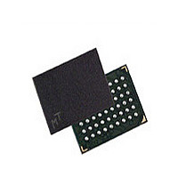
MT45W8MW16BGX-701 IT Micron Technology Inc, MT45W8MW16BGX-701 IT Datasheet - Page 15

MT45W8MW16BGX-701 IT
Manufacturer Part Number
MT45W8MW16BGX-701 IT
Description
Manufacturer
Micron Technology Inc
Datasheet
1.MT45W8MW16BGX-701_IT.pdf
(68 pages)
Specifications of MT45W8MW16BGX-701 IT
Operating Temperature (max)
85C
Operating Temperature (min)
-40C
Mounting
Surface Mount
Operating Temperature Classification
Industrial
Lead Free Status / RoHS Status
Compliant
Mixed-Mode Operation
WAIT Operation
Figure 10:
PDF: 09005aef80ec6f79/Source: 09005aef80ec6f65
128mb_burst_cr1_5_p26z__2.fm - Rev. H 9/07 EN
Wired-OR WAIT Configuration
The device supports a combination of synchronous READ and asynchronous READ and
WRITE operations when the BCR is configured for synchronous operation. The asyn-
chronous READ and WRITE operations require that the clock (CLK) remain LOW during
the entire sequence. The ADV# signal can be used to latch the target address, or it can
remain LOW during the entire WRITE operation. CE# can remain LOW when transi-
tioning between mixed-mode operations with fixed latency enabled; however, the CE#
LOW time must not exceed
to legacy burst mode Flash memory controllers. See Figure 50 on page 62 for the “Asyn-
chronous WRITE Followed by Burst READ” timing diagram.
The WAIT output on a CellularRAM device is typically connected to a shared, system-
level WAIT signal. (See Figure 10.) The shared WAIT signal is used by the processor to
coordinate transactions with multiple memories on the synchronous bus.
Once a READ or WRITE operation has been initiated, WAIT goes active to indicate that
the CellularRAM device requires additional time before data can be transferred. For
READ operations, WAIT will remain active until valid data is output from the device. For
WRITE operations, WAIT will indicate to the memory controller when data will be
accepted into the CellularRAM device. When WAIT transitions to an inactive state, the
data burst will progress on successive clock edges.
During a burst cycle, CE# must remain asserted until the first data is valid. Bringing CE#
high during this initial latency may cause data corruption.
When using variable initial access latency (BCR[14] = 0), the WAIT output performs an
arbitration role for READ operations launched while an on-chip refresh is in progress. If
a collision occurs, WAIT is asserted for additional clock cycles until the refresh has
completed. (See Figure 11 on page 16.) When the refresh operation has completed, the
READ operation will continue normally.
WAIT will be asserted but should be ignored during asynchronous READ, WRITE, and
page READ operations.
By using fixed initial latency (BCR[14] = 1), this CellularRAM device can be used in burst
mode without monitoring the WAIT signal. However, WAIT can still be used to deter-
mine when valid data is available at the start of the burst and at the end of the row. If
WAIT is not monitored, the controller must stop burst accesses at row boundaries on its
own.
Processor
READY
128Mb: 8 Meg x 16 Async/Page/Burst CellularRAM 1.5 Async/
WAIT
device
Other
CellularRAM
WAIT
t
CEM. Mixed-mode operation facilitates a seamless interface
15
WAIT
device
Other
Micron Technology, Inc., reserves the right to change products or specifications without notice.
External
pull-up/
pull-down
resistor
Page/Burst CellularRAM 1.5 Memory
©2004 Micron Technology, Inc. All rights reserved.


