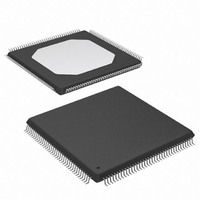
XCS10XL-5TQ144C Xilinx Inc, XCS10XL-5TQ144C Datasheet - Page 11

XCS10XL-5TQ144C
Manufacturer Part Number
XCS10XL-5TQ144C
Description
IC FPGA 3.3V C-TEMP 144-TQFP
Manufacturer
Xilinx Inc
Series
Spartan™-XLr
Datasheet
1.XCS05XL-4VQG100C.pdf
(83 pages)
Specifications of XCS10XL-5TQ144C
Number Of Logic Elements/cells
466
Number Of Labs/clbs
196
Total Ram Bits
6272
Number Of I /o
112
Number Of Gates
10000
Voltage - Supply
3 V ~ 3.6 V
Mounting Type
Surface Mount
Operating Temperature
0°C ~ 85°C
Package / Case
144-LQFP
Case
TQFP144
Dc
02+
Lead Free Status / RoHS Status
Contains lead / RoHS non-compliant
Available stocks
Company
Part Number
Manufacturer
Quantity
Price
Company:
Part Number:
XCS10XL-5TQ144C
Manufacturer:
XILINX
Quantity:
5 530
Company:
Part Number:
XCS10XL-5TQ144C
Manufacturer:
SMD
Quantity:
246
Company:
Part Number:
XCS10XL-5TQ144C
Manufacturer:
XILINX
Quantity:
23
CLB Interface
A block diagram of the CLB interface signals is shown in
Figure
on all four sides providing maximum routing flexibility. In
general, the entire architecture is symmetrical and regular.
It is well suited to established placement and routing algo-
rithms. Inputs, outputs, and function generators can freely
swap positions within a CLB to avoid routing congestion
during the placement and routing operation. The exceptions
are the clock (K) input and CIN/COUT signals. The K input
is routed to dedicated global vertical lines as well as four
single-length lines and is on the left side of the CLB. The
CIN/COUT signals are routed through dedicated intercon-
nects which do not interfere with the general routing struc-
ture. The output signals from the CLB are available to drive
both vertical and horizontal channels.
DS060 (v1.8) June 26, 2008
Product Specification
COUT
9. The input signals to the CLB are distributed evenly
CIN
G1
C1
F1
K
X
Figure 9: CLB Interconnect Signals
R
Figure 8: Spartan/XL CLB Routing Channels and Interface Block Diagram
CLB
PSM
PSM
2 Doubles
Rev 1.1
DS060_08_081100
CLB
3 Longs
Y
G3
C3
F3
www.xilinx.com
8 Singles
PSM
PSM
3 Longs
Programmable Switch Matrices
The horizontal and vertical single- and double-length lines
intersect at a box called a programmable switch matrix
(PSM). Each PSM consists of programmable pass transis-
tors used to establish connections between the lines (see
Figure
For example, a single-length signal entering on the right
side of the switch matrix can be routed to a single-length
line on the top, left, or bottom sides, or any combination
thereof, if multiple branches are required. Similarly, a dou-
ble-length signal can be routed to a double-length line on
any or all of the other three edges of the programmable
switch matrix.
Single-Length Lines
Single-length lines provide the greatest interconnect flexibil-
ity and offer fast routing between adjacent blocks. There are
eight vertical and eight horizontal single-length lines associ-
ated with each CLB. These lines connect the switching
matrices that are located in every row and column of CLBs.
Single-length lines are connected by way of the program-
mable switch matrices, as shown in
nectivity is shown in
Single-length lines incur a delay whenever they go through
a PSM. Therefore, they are not suitable for routing signals
for long distances. They are normally used to conduct sig-
nals within a localized area and to provide the branching for
nets with fanout greater than one.
CLB
Spartan and Spartan-XL FPGA Families Data Sheet
10).
2 Doubles
PSM
PSM
Figure
DS060_09_041901
8 Singles
2 Doubles
3 Longs
3 Longs
2 Doubles
8.
Figure
10. Routing con-
11


