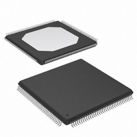
XCS10XL-5TQ144C Xilinx Inc, XCS10XL-5TQ144C Datasheet - Page 6

XCS10XL-5TQ144C
Manufacturer Part Number
XCS10XL-5TQ144C
Description
IC FPGA 3.3V C-TEMP 144-TQFP
Manufacturer
Xilinx Inc
Series
Spartan™-XLr
Datasheet
1.XCS05XL-4VQG100C.pdf
(83 pages)
Specifications of XCS10XL-5TQ144C
Number Of Logic Elements/cells
466
Number Of Labs/clbs
196
Total Ram Bits
6272
Number Of I /o
112
Number Of Gates
10000
Voltage - Supply
3 V ~ 3.6 V
Mounting Type
Surface Mount
Operating Temperature
0°C ~ 85°C
Package / Case
144-LQFP
Case
TQFP144
Dc
02+
Lead Free Status / RoHS Status
Contains lead / RoHS non-compliant
Available stocks
Company
Part Number
Manufacturer
Quantity
Price
Company:
Part Number:
XCS10XL-5TQ144C
Manufacturer:
XILINX
Quantity:
5 530
Company:
Part Number:
XCS10XL-5TQ144C
Manufacturer:
SMD
Quantity:
246
Company:
Part Number:
XCS10XL-5TQ144C
Manufacturer:
XILINX
Quantity:
23
Spartan and Spartan-XL FPGA Families Data Sheet
The four internal control signals are:
•
•
•
•
Input/Output Blocks (IOBs)
User-configurable input/output blocks (IOBs) provide the
interface between external package pins and the internal
logic. Each IOB controls one package pin and can be con-
figured for input, output, or bidirectional signals.
shows a simplified functional block diagram of the Spar-
tan/XL FPGA IOB.
6
EC: Enable Clock
SR: Asynchronous Set/Reset or H function generator
Input 0
DIN: Direct In or H function generator Input 2
H1: H function generator Input 1.
Figure 4: CLB Control Signal Interface
C1
C2
C3
C4
Multiplexer Controlled
by Configuration Program
DS060_04_081100
DIN
H1
SR
EC
Figure 6
www.xilinx.com
IOB Input Signal Path
The input signal to the IOB can be configured to either go
directly to the routing channels (via I1 and I2 in
to the input register. The input register can be programmed
as either an edge-triggered flip-flop or a level-sensitive
latch. The functionality of this register is shown in
and a simplified block diagram of the register can be seen in
Figure
Table 3: Input Register Functionality
Power-Up or
GSR
Flip-Flop
Latch
Both
Figure 5: IOB Flip-Flop/Latch Functional Block
Legend:
5.
Mode
SR
CK
EC
0*
1*
X
D
Vcc
Don’t care.
Rising edge (clock not inverted).
Set or Reset value. Reset is default.
Input is Low or unconnected (default
value)
Input is High or unconnected (default
value)
CK
GSR
Diagram
X
X
0
1
0
Multiplexer Controlled
by Configuration Program
DS060 (v1.8) June 26, 2008
D
EC
1*
1*
1*
X
X
0
RD
SD
Product Specification
DS060_05_041901
Q
D
X
D
X
X
D
X
Figure
Q
Table
SR
Q
D
Q
Q
D
Q
6) or
3,
R


