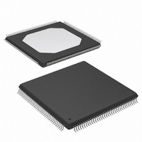
XCS10XL-5TQ144C Xilinx Inc, XCS10XL-5TQ144C Datasheet - Page 39

XCS10XL-5TQ144C
Manufacturer Part Number
XCS10XL-5TQ144C
Description
IC FPGA 3.3V C-TEMP 144-TQFP
Manufacturer
Xilinx Inc
Series
Spartan™-XLr
Datasheet
1.XCS05XL-4VQG100C.pdf
(83 pages)
Specifications of XCS10XL-5TQ144C
Number Of Logic Elements/cells
466
Number Of Labs/clbs
196
Total Ram Bits
6272
Number Of I /o
112
Number Of Gates
10000
Voltage - Supply
3 V ~ 3.6 V
Mounting Type
Surface Mount
Operating Temperature
0°C ~ 85°C
Package / Case
144-LQFP
Case
TQFP144
Dc
02+
Lead Free Status / RoHS Status
Contains lead / RoHS non-compliant
Available stocks
Company
Part Number
Manufacturer
Quantity
Price
Company:
Part Number:
XCS10XL-5TQ144C
Manufacturer:
XILINX
Quantity:
5 530
Company:
Part Number:
XCS10XL-5TQ144C
Manufacturer:
SMD
Quantity:
246
Company:
Part Number:
XCS10XL-5TQ144C
Manufacturer:
XILINX
Quantity:
23
Readback Abort
When the Readback Abort option is selected, a High-to-Low
transition on RDBK.TRIG terminates the Readback opera-
tion and prepares the logic to accept another trigger.
After an aborted Readback, additional clocks (up to one
Readback clock per configuration frame) may be required to
re-initialize the control logic. The status of Readback is indi-
cated by the output control net RDBK.RIP. RDBK.RIP is
High whenever a readback is in progress.
Clock Select
CCLK is the default clock. However, the user can insert
another clock on RDBK.CLK. Readback control and data
are clocked on rising edges of RDBK.CLK. If Readback
must be inhibited for security reasons, the Readback control
nets are simply not connected. RDBK.CLK is located in the
lower right chip corner.
Violating the Maximum High and Low Time
Specification for the Readback Clock
The Readback clock has a maximum High and Low time
specification. In some cases, this specification cannot be
DS060 (v1.8) June 26, 2008
Product Specification
R
www.xilinx.com
met. For example, if a processor is controlling Readback, an
interrupt may force it to stop in the middle of a readback.
This necessitates stopping the clock, and thus violating the
specification.
The specification is mandatory only on clocking data at the
end of a frame prior to the next start bit. The transfer mech-
anism will load the data to a shift register during the last six
clock cycles of the frame, prior to the start bit of the following
frame. This loading process is dynamic, and is the source of
the maximum High and Low time requirements.
Therefore, the specification only applies to the six clock
cycles prior to and including any start bit, including the
clocks before the first start bit in the Readback data stream.
At other times, the frame data is already in the register and
the register is not dynamic. Thus, it can be shifted out just
like a regular shift register.
The user must precisely calculate the location of the Read-
back data relative to the frame. The system must keep track
of the position within a data frame, and disable interrupts
before frame boundaries. Frame lengths and data formats
are listed in
Spartan and Spartan-XL FPGA Families Data Sheet
Table 16
and
Table
17.
39


