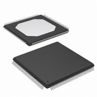
XCS10XL-5TQ144C Xilinx Inc, XCS10XL-5TQ144C Datasheet - Page 43

XCS10XL-5TQ144C
Manufacturer Part Number
XCS10XL-5TQ144C
Description
IC FPGA 3.3V C-TEMP 144-TQFP
Manufacturer
Xilinx Inc
Series
Spartan™-XLr
Datasheet
1.XCS05XL-4VQG100C.pdf
(83 pages)
Specifications of XCS10XL-5TQ144C
Number Of Logic Elements/cells
466
Number Of Labs/clbs
196
Total Ram Bits
6272
Number Of I /o
112
Number Of Gates
10000
Voltage - Supply
3 V ~ 3.6 V
Mounting Type
Surface Mount
Operating Temperature
0°C ~ 85°C
Package / Case
144-LQFP
Case
TQFP144
Dc
02+
Lead Free Status / RoHS Status
Contains lead / RoHS non-compliant
Available stocks
Company
Part Number
Manufacturer
Quantity
Price
Company:
Part Number:
XCS10XL-5TQ144C
Manufacturer:
XILINX
Quantity:
5 530
Company:
Part Number:
XCS10XL-5TQ144C
Manufacturer:
SMD
Quantity:
246
Company:
Part Number:
XCS10XL-5TQ144C
Manufacturer:
XILINX
Quantity:
23
Spartan Family DC Characteristics Over Operating Conditions
Spartan Family Global Buffer Switching Characteristic Guidelines
All devices are 100% functionally tested. Internal timing
parameters are derived from measuring internal test pat-
terns. Listed below are representative values where one
global clock input drives one vertical clock line in each
accessible column, and where all accessible IOB and CLB
flip-flops are clocked by the global clock net.
When fewer vertical clock lines are connected, the clock dis-
tribution is faster; when multiple clock lines per column are
driven from the same global clock, the delay is longer. For
DS060 (v1.8) June 26, 2008
Product Specification
Notes:
1.
2.
Symbol
Symbol
With 50% of the outputs simultaneously sinking 12 mA, up to a maximum of 64 pins.
With no output current loads, no active input pull-up resistors, all package pins at V
option.
I
I
I
V
V
T
T
V
CCO
C
RPU
RPD
I
OH
PG
SG
OL
DR
L
IN
R
High-level output voltage @ I
High-level output voltage @ I
Low-level output voltage @ I
Data retention supply voltage (below which configuration data may be lost)
Quiescent FPGA supply current
Input or output leakage current
Input capacitance (sample tested)
Pad pull-up (when selected) @ V
Pad pull-down (when selected) @ V
From pad through Primary buffer, to any clock K
From pad through Secondary buffer, to any clock K
Description
OL
OH
OH
= 12.0 mA, V
Description
(2)
= –4.0 mA, V
= –1.0 mA, V
IN
= 0V (sample tested)
IN
= 5V (sample tested)
www.xilinx.com
CC
CC
CC
min
min
min
more specific, more precise, and worst-case guaranteed
data, reflecting the actual routing structure, use the values
provided by the static timing analyzer (TRCE in the Xilinx
Development System) and back-annotated to the simulation
netlist. These path delays, provided as a guideline, have
been extracted from the static timing analyzer report. All
timing parameters assume worst-case operating conditions
(supply voltage and junction temperature).
(1)
Spartan and Spartan-XL FPGA Families Data Sheet
TTL outputs
CMOS outputs
TTL outputs
CMOS outputs
Commercial
Industrial
Device
XCS05
XCS10
XCS20
XCS30
XCS40
XCS05
XCS10
XCS20
XCS30
XCS40
CC
or GND, and the FPGA configured with a Tie
Max
2.0
2.4
2.8
3.2
3.5
2.5
2.9
3.3
3.6
3.9
-4
Speed Grade
V
CC
0.02
0.02
Min
–10
2.4
3.0
-
-
-
-
-
– 0.5
Max
4.0
4.3
5.4
5.8
6.4
4.4
4.7
5.8
6.2
6.7
-3
Max
0.25
+10
0.4
0.4
3.0
6.0
10
-
-
-
-
Units
Units
mA
mA
mA
mA
μA
pF
V
V
V
V
V
ns
ns
ns
ns
ns
ns
ns
ns
ns
ns
43


