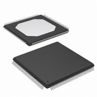
XCS10XL-5TQ144C Xilinx Inc, XCS10XL-5TQ144C Datasheet - Page 27

XCS10XL-5TQ144C
Manufacturer Part Number
XCS10XL-5TQ144C
Description
IC FPGA 3.3V C-TEMP 144-TQFP
Manufacturer
Xilinx Inc
Series
Spartan™-XLr
Datasheet
1.XCS05XL-4VQG100C.pdf
(83 pages)
Specifications of XCS10XL-5TQ144C
Number Of Logic Elements/cells
466
Number Of Labs/clbs
196
Total Ram Bits
6272
Number Of I /o
112
Number Of Gates
10000
Voltage - Supply
3 V ~ 3.6 V
Mounting Type
Surface Mount
Operating Temperature
0°C ~ 85°C
Package / Case
144-LQFP
Case
TQFP144
Dc
02+
Lead Free Status / RoHS Status
Contains lead / RoHS non-compliant
Available stocks
Company
Part Number
Manufacturer
Quantity
Price
Company:
Part Number:
XCS10XL-5TQ144C
Manufacturer:
XILINX
Quantity:
5 530
Company:
Part Number:
XCS10XL-5TQ144C
Manufacturer:
SMD
Quantity:
246
Company:
Part Number:
XCS10XL-5TQ144C
Manufacturer:
XILINX
Quantity:
23
Master Serial Mode
The Master serial mode uses an internal oscillator to gener-
ate a Configuration Clock (CCLK) for driving potential slave
devices
(SPROM). The CCLK speed is selectable as either 1 MHz
(default) or 8 MHz. Configuration always starts at the default
slow frequency, then can switch to the higher frequency dur-
ing the first frame. Frequency tolerance is –50% to +25%.
In Master Serial mode, the CCLK output of the device drives
a Xilinx SPROM that feeds the FPGA DIN input. Each rising
edge of the CCLK output increments the Serial PROM inter-
nal address counter. The next data bit is put on the SPROM
data output, connected to the FPGA DIN pin. The FPGA
accepts this data on the subsequent rising CCLK edge.
When used in a daisy-chain configuration the Master Serial
FPGA is placed as the first device in the chain and is
referred to as the lead FPGA. The lead FPGA presents the
preamble data, and all data that overflows the lead device,
on its DOUT pin. There is an internal pipeline delay of 1.5
CCLK periods, which means that DOUT changes on the
Slave Serial Mode
In Slave Serial mode, the FPGA receives serial configura-
tion data on the rising edge of CCLK and, after loading its
configuration, passes additional data out, resynchronized
on the next falling edge of CCLK.
In this mode, an external signal drives the CCLK input of the
FPGA (most often from a Master Serial device). The serial
configuration bitstream must be available at the DIN input of
the lead FPGA a short setup time before each rising CCLK
edge.
DS060 (v1.8) June 26, 2008
Product Specification
and
R
Serial Data In
Serial DOUT
the
(Output)
(Output)
CCLK
Xilinx
Notes:
1.
2.
Figure 24: Master Serial Mode Programming Switching Characteristics
CCLK
At power-up, V
delay configuration by pulling PROGRAM Low until V
Master Serial mode timing is based on testing in slave mode.
serial-configuration
n – 3
T
T
Symbol
DSCK
CKDS
T
DSCK
CC
n
must rise from 2.0V to V
DIN setup
DIN hold
n – 2
PROM
www.xilinx.com
Description
T
CKDS
n + 1
falling CCLK edge, and the next FPGA in the daisy chain
accepts data on the subsequent rising CCLK edge. See the
timing diagram in
In the bitstream generation software, the user can specify
Fast Configuration Rate, which, starting several bits into the
first frame, increases the CCLK frequency by a factor of
eight. For actual timing values please refer to the specifica-
tion section. Be sure that the serial PROM and slaves are
fast enough to support this data rate. Earlier families such
as the XC3000 series do not support the Fast Configuration
Rate option.
The SPROM CE input can be driven from either LDC or
DONE. Using LDC avoids potential contention on the DIN
pin, if this pin is configured as user I/O, but LDC is then
restricted to be a permanently High user output after config-
uration. Using DONE can also avoid contention on DIN, pro-
vided the Early DONE option is invoked.
Figure 25
device is in Master Serial mode, all other devices in the
chain are in Slave Serial mode.
The lead FPGA then presents the preamble data—and all
data that overflows the lead device—on its DOUT pin. There
is an internal delay of 0.5 CCLK periods, which means that
DOUT changes on the falling CCLK edge, and the next
FPGA in the daisy chain accepts data on the subsequent
rising CCLK edge.
Figure 25
device in Slave Serial mode should be connected as shown
in the third device from the left.
CC
Spartan and Spartan-XL FPGA Families Data Sheet
min in less than 25 ms, otherwise
n – 1
shows a full master/slave system. A Spartan/XL
shows a full master/slave system. The leftmost
CC
is valid.
Figure
n + 2
Min
20
0
24.
Units
ns
ns
n
DS060_24_080400
27


