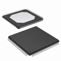
XCS10XL-5TQ144C Xilinx Inc, XCS10XL-5TQ144C Datasheet - Page 20

XCS10XL-5TQ144C
Manufacturer Part Number
XCS10XL-5TQ144C
Description
IC FPGA 3.3V C-TEMP 144-TQFP
Manufacturer
Xilinx Inc
Series
Spartan™-XLr
Datasheet
1.XCS05XL-4VQG100C.pdf
(83 pages)
Specifications of XCS10XL-5TQ144C
Number Of Logic Elements/cells
466
Number Of Labs/clbs
196
Total Ram Bits
6272
Number Of I /o
112
Number Of Gates
10000
Voltage - Supply
3 V ~ 3.6 V
Mounting Type
Surface Mount
Operating Temperature
0°C ~ 85°C
Package / Case
144-LQFP
Case
TQFP144
Dc
02+
Lead Free Status / RoHS Status
Contains lead / RoHS non-compliant
Available stocks
Company
Part Number
Manufacturer
Quantity
Price
Company:
Part Number:
XCS10XL-5TQ144C
Manufacturer:
XILINX
Quantity:
5 530
Company:
Part Number:
XCS10XL-5TQ144C
Manufacturer:
SMD
Quantity:
246
Company:
Part Number:
XCS10XL-5TQ144C
Manufacturer:
XILINX
Quantity:
23
Spartan and Spartan-XL FPGA Families Data Sheet
On-Chip Oscillator
Spartan/XL devices include an internal oscillator. This oscil-
lator is used to clock the power-on time-out, for configura-
tion memory clearing, and as the source of CCLK in Master
configuration mode. The oscillator runs at a nominal 8 MHz
frequency that varies with process, V
The output frequency falls between 4 MHz and 10 MHz.
The oscillator output is optionally available after configura-
tion. Any two of four resynchronized taps of a built-in divider
are also available. These taps are at the fourth, ninth, four-
teenth and nineteenth bits of the divider. Therefore, if the
primary oscillator output is running at the nominal 8 MHz,
the user has access to an 8-MHz clock, plus any two of
500 kHz, 16 kHz, 490 Hz and 15 Hz. These frequencies
can vary by as much as -50% or +25%.
These signals can be accessed by placing the OSC4 library
element in a schematic or in HDL code. The oscillator is
automatically disabled after configuration if the OSC4 sym-
bol is not used in the design.
Global Signals: GSR and GTS
Global Set/Reset
A separate Global Set/Reset line, as shown in
page 5
clears each flip-flop during power-up, reconfiguration, or
when a dedicated Reset net is driven active. This global net
(GSR) does not compete with other routing resources; it
uses a dedicated distribution network.
Each flip-flop is configured as either globally set or reset in
the same way that the local set/reset (SR) is specified.
Therefore, if a flip-flop is set by SR, it is also set by GSR.
Similarly, if in reset mode, it is reset by both SR and GSR.
GSR can be driven from any user-programmable pin as a
global reset input. To use this global net, place an input pad
and input buffer in the schematic or HDL code, driving the
GSR pin of the STARTUP symbol. (See
cific pin location can be assigned to this input using a LOC
attribute or property, just as with any other user-program-
mable pad. An inverter can optionally be inserted after the
input buffer to invert the sense of the GSR signal. Alterna-
tively, GSR can be driven from any internal node.
Global 3-State
A separate Global 3-state line (GTS) as shown in
page 7
state, unless boundary scan is enabled and is executing an
EXTEST instruction. GTS does not compete with other rout-
ing resources; it uses a dedicated distribution network.
GTS can be driven from any user-programmable pin as a
global 3-state input. To use this global net, place an input
pad and input buffer in the schematic or HDL code, driving
the GTS pin of the STARTUP symbol. This is similar to what
is shown in
20
for the CLB and
forces all FPGA outputs to the high-impedance
Figure 19
for GSR except the IBUF would be
Figure 5, page 6
CC
, and temperature.
for the IOB, sets or
Figure
19.) A spe-
Figure 3,
Figure 6,
www.xilinx.com
connected to GTS. A specific pin location can be assigned
to this input using a LOC attribute or property, just as with
any other user-programmable pad. An inverter can option-
ally be inserted after the input buffer to invert the sense of
the Global 3-state signal. Alternatively, GTS can be driven
from any internal node.
Boundary Scan
The "bed of nails" has been the traditional method of testing
electronic assemblies. This approach has become less
appropriate, due to closer pin spacing and more sophisti-
cated assembly methods like surface-mount technology
and multi-layer boards. The IEEE Boundary Scan Standard
1149.1 was developed to facilitate board-level testing of
electronic assemblies. Design and test engineers can
embed a standard test logic structure in their device to
achieve high fault coverage for I/O and internal logic. This
structure is easily implemented with a four-pin interface on
any boundary scan compatible device. IEEE 1149.1-com-
patible devices may be serial daisy-chained together, con-
nected in parallel, or a combination of the two.
The Spartan and Spartan-XL families implement IEEE
1149.1-compatible BYPASS, PRELOAD/SAMPLE and
EXTEST boundary scan instructions. When the boundary
scan configuration option is selected, three normal user I/O
pins become dedicated inputs for these functions. Another
user output pin becomes the dedicated boundary scan out-
put. The details of how to enable this circuitry are covered
later in this section.
By exercising these input signals, the user can serially load
commands and data into these devices to control the driving
of their outputs and to examine their inputs. This method is
an improvement over bed-of-nails testing. It avoids the need
to over-drive device outputs, and it reduces the user inter-
face to four pins. An optional fifth pin, a reset for the control
logic, is described in the standard but is not implemented in
the Spartan/XL devices.
The dedicated on-chip logic implementing the IEEE 1149.1
functions includes a 16-state machine, an instruction regis-
ter and a number of data registers. The functional details
can be found in the IEEE 1149.1 specification and are also
discussed in the Xilinx application note: "Boundary Scan in
FPGA Devices."
PAD
Figure 19: Symbols for Global Set/Reset
IBUF
DS060 (v1.8) June 26, 2008
GSR
GTS
CLK
Product Specification
STARTUP
DONEIN
Q1, Q4
DS060_19_080400
Q2
Q3
R


