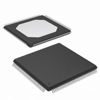
XCS10XL-5TQ144C Xilinx Inc, XCS10XL-5TQ144C Datasheet - Page 63

XCS10XL-5TQ144C
Manufacturer Part Number
XCS10XL-5TQ144C
Description
IC FPGA 3.3V C-TEMP 144-TQFP
Manufacturer
Xilinx Inc
Series
Spartan™-XLr
Datasheet
1.XCS05XL-4VQG100C.pdf
(83 pages)
Specifications of XCS10XL-5TQ144C
Number Of Logic Elements/cells
466
Number Of Labs/clbs
196
Total Ram Bits
6272
Number Of I /o
112
Number Of Gates
10000
Voltage - Supply
3 V ~ 3.6 V
Mounting Type
Surface Mount
Operating Temperature
0°C ~ 85°C
Package / Case
144-LQFP
Case
TQFP144
Dc
02+
Lead Free Status / RoHS Status
Contains lead / RoHS non-compliant
Available stocks
Company
Part Number
Manufacturer
Quantity
Price
Company:
Part Number:
XCS10XL-5TQ144C
Manufacturer:
XILINX
Quantity:
5 530
Company:
Part Number:
XCS10XL-5TQ144C
Manufacturer:
SMD
Quantity:
246
Company:
Part Number:
XCS10XL-5TQ144C
Manufacturer:
XILINX
Quantity:
23
Table 18: Pin Descriptions (Continued)
DS060 (v1.8) June 26, 2008
Product Specification
User I/O Pins That Can Have Special Functions
PWRDWN
Pin Name
TDI, TCK,
(Spartan)
PGCK1 -
PGCK4
TDO
TMS
HDC
LDC
INIT
R
Config.
During
Pull-up
Weak
I/O
I/O
O
O
O
I
I
I/O After
Config.
(JTAG)
I or I/O
or I
I/O
I/O
I/O
I/O
O
I
PWRDWN is an active Low input that forces the FPGA into the Power Down state
and reduces power consumption. When PWRDWN is Low, the FPGA disables all
I/O and initializes all flip-flops. All inputs are interpreted as Low independent of
their actual level. VCC must be maintained, and the configuration data is
maintained. PWRDWN halts configuration if asserted before or during
configuration, and re-starts configuration when removed. When PWRDWN returns
High, the FPGA becomes operational by first enabling the inputs and flip-flops and
then enabling the outputs. PWRDWN has a default internal pull-up resistor.
If boundary scan is used, this pin is the Test Data Output. If boundary scan is not
used, this pin is a 3-state output without a register, after configuration is
completed.
To use this pin, place the library component TDO instead of the usual pad symbol.
An output buffer must still be used.
If boundary scan is used, these pins are Test Data In, Test Clock, and Test Mode
Select inputs respectively. They come directly from the pads, bypassing the IOBs.
These pins can also be used as inputs to the CLB logic after configuration is
completed.
If the BSCAN symbol is not placed in the design, all boundary scan functions are
inhibited once configuration is completed, and these pins become
user-programmable I/O. In this case, they must be called out by special library
elements. To use these pins, place the library components TDI, TCK, and TMS
instead of the usual pad symbols. Input or output buffers must still be used.
High During Configuration (HDC) is driven High until the I/O go active. It is
available as a control output indicating that configuration is not yet completed.
After configuration, HDC is a user-programmable I/O pin.
Low During Configuration (LDC) is driven Low until the I/O go active. It is available
as a control output indicating that configuration is not yet completed. After
configuration, LDC is a user-programmable I/O pin.
Before and during configuration, INIT is a bidirectional signal. A 1 kΩ to 10 kΩ
external pull-up resistor is recommended.
As an active Low open-drain output, INIT is held Low during the power stabilization
and internal clearing of the configuration memory. As an active Low input, it can
be used to hold the FPGA in the internal WAIT state before the start of
configuration. Master mode devices stay in a WAIT state an additional 30 to
300 μs after INIT has gone High.
During configuration, a Low on this output indicates that a configuration data error
has occurred. After the I/O go active, INIT is a user-programmable I/O pin.
Four Primary Global inputs each drive a dedicated internal global net with short
delay and minimal skew. If not used to drive a global buffer, any of these pins is a
user-programmable I/O.
The PGCK1-PGCK4 pins drive the four Primary Global Buffers. Any input pad
symbol connected directly to the input of a BUFGP symbol is automatically placed
on one of these pins.
www.xilinx.com
Spartan and Spartan-XL FPGA Families Data Sheet
Pin Description
63


