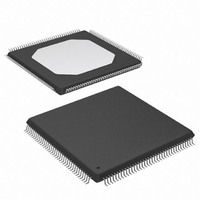
XCS10XL-5TQ144C Xilinx Inc, XCS10XL-5TQ144C Datasheet - Page 21

XCS10XL-5TQ144C
Manufacturer Part Number
XCS10XL-5TQ144C
Description
IC FPGA 3.3V C-TEMP 144-TQFP
Manufacturer
Xilinx Inc
Series
Spartan™-XLr
Datasheet
1.XCS05XL-4VQG100C.pdf
(83 pages)
Specifications of XCS10XL-5TQ144C
Number Of Logic Elements/cells
466
Number Of Labs/clbs
196
Total Ram Bits
6272
Number Of I /o
112
Number Of Gates
10000
Voltage - Supply
3 V ~ 3.6 V
Mounting Type
Surface Mount
Operating Temperature
0°C ~ 85°C
Package / Case
144-LQFP
Case
TQFP144
Dc
02+
Lead Free Status / RoHS Status
Contains lead / RoHS non-compliant
Available stocks
Company
Part Number
Manufacturer
Quantity
Price
Company:
Part Number:
XCS10XL-5TQ144C
Manufacturer:
XILINX
Quantity:
5 530
Company:
Part Number:
XCS10XL-5TQ144C
Manufacturer:
SMD
Quantity:
246
Company:
Part Number:
XCS10XL-5TQ144C
Manufacturer:
XILINX
Quantity:
23
Figure 20
scan logic. It includes three bits of Data Register per IOB,
the IEEE 1149.1 Test Access Port controller, and the
Instruction Register with decodes.
Spartan/XL devices can also be configured through the
boundary scan logic. See
Boundary Scan Pins, page
Data Registers
The primary data register is the boundary scan register. For
each IOB pin in the FPGA, bonded or not, it includes three
bits for In, Out and 3-state Control. Non-IOB pins have
appropriate partial bit population for In or Out only. PRO-
GRAM, CCLK and DONE are not included in the boundary
scan register. Each EXTEST CAPTURE-DR state captures
all In, Out, and 3-state pins.
The data register also includes the following non-pin bits:
TDO.T, and TDO.O, which are always bits 0 and 1 of the
data register, respectively, and BSCANT.UPD, which is
always the last bit of the data register. These three bound-
ary scan bits are special-purpose Xilinx test signals.
DS060 (v1.8) June 26, 2008
Product Specification
is a diagram of the Spartan/XL FPGA boundary
R
37.
Configuration Through the
www.xilinx.com
The other standard data register is the single flip-flop
BYPASS register. It synchronizes data being passed
through the FPGA to the next downstream boundary scan
device.
The FPGA provides two additional data registers that can
be specified using the BSCAN macro. The FPGA provides
two user pins (BSCAN.SEL1 and BSCAN.SEL2) which are
the decodes of two user instructions. For these instructions,
two corresponding pins (BSCAN.TDO1 and BSCAN.TDO2)
allow user scan data to be shifted out on TDO. The data
register clock (BSCAN.DRCK) is available for control of test
logic which the user may wish to implement with CLBs. The
NAND of TCK and RUN-TEST-IDLE is also provided
(BSCAN.IDLE).
Instruction Set
The Spartan/XL FPGA boundary scan instruction set also
includes instructions to configure the device and read back
the configuration data. The instruction set is coded as
shown in
Spartan and Spartan-XL FPGA Families Data Sheet
Table
12.
21


