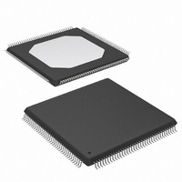
XCS10XL-5TQ144C Xilinx Inc, XCS10XL-5TQ144C Datasheet - Page 7

XCS10XL-5TQ144C
Manufacturer Part Number
XCS10XL-5TQ144C
Description
IC FPGA 3.3V C-TEMP 144-TQFP
Manufacturer
Xilinx Inc
Series
Spartan™-XLr
Datasheet
1.XCS05XL-4VQG100C.pdf
(83 pages)
Specifications of XCS10XL-5TQ144C
Number Of Logic Elements/cells
466
Number Of Labs/clbs
196
Total Ram Bits
6272
Number Of I /o
112
Number Of Gates
10000
Voltage - Supply
3 V ~ 3.6 V
Mounting Type
Surface Mount
Operating Temperature
0°C ~ 85°C
Package / Case
144-LQFP
Case
TQFP144
Dc
02+
Lead Free Status / RoHS Status
Contains lead / RoHS non-compliant
Available stocks
Company
Part Number
Manufacturer
Quantity
Price
Company:
Part Number:
XCS10XL-5TQ144C
Manufacturer:
XILINX
Quantity:
5 530
Company:
Part Number:
XCS10XL-5TQ144C
Manufacturer:
SMD
Quantity:
246
Company:
Part Number:
XCS10XL-5TQ144C
Manufacturer:
XILINX
Quantity:
23
The register choice is made by placing the appropriate
library symbol. For example, IFD is the basic input flip-flop
(rising edge triggered), and ILD is the basic input latch
(transparent-High). Variations with inverted clocks are also
available. The clock signal inverter is also shown in
on the CK line.
The Spartan family IOB data input path has a one-tap delay
element: either the delay is inserted (default), or it is not.
The Spartan-XL family IOB data input path has a two-tap
delay element, with choices of a full delay, a partial delay, or
no delay. The added delay guarantees a zero hold time with
respect to clocks routed through the global clock buffers.
(See
the global clock buffers in the Spartan/XL families.) For a
shorter input register setup time, with positive hold-time,
attach a NODELAY attribute or property to the flip-flop.The
output of the input register goes to the routing channels (via
I1 and I2 in
can each carry either the direct or registered input signal.
The 5V Spartan family input buffers can be globally config-
ured for either TTL (1.2V) or CMOS (VCC/2) thresholds,
DS060 (v1.8) June 26, 2008
Product Specification
Global Nets and Buffers, page 12
OK
Figure
EC
R
IK
O
I1
I2
T
6). The I1 and I2 signals that exit the IOB
Figure 6: Simplified Spartan/XL IOB Block Diagram
D
CK
EC
D
CK
EC
for a description of
GTS
Q
Q
Figure 5
www.xilinx.com
Multiplexer Controlled
by Configuration Program
Programmable TTL/CMOS Drive
using an option in the bitstream generation software. The
Spartan family output levels are also configurable; the two
global adjustments of input threshold and output level are
independent. The inputs of Spartan devices can be driven
by the outputs of any 3.3V device, if the Spartan family
inputs are in TTL mode. Input and output thresholds are
TTL on all configuration pins until the configuration has
been loaded into the device and specifies how they are to
be used. Spartan-XL family inputs are TTL compatible and
3.3V CMOS compatible.
Supported sources for Spartan/XL device inputs are shown
in
Spartan-XL family I/Os are fully 5V tolerant even though the
V
Spartan-XL family inputs without damage, as shown in
Table
after 5V signals are applied to the I/Os. This makes the
Spartan-XL devices immune to power supply sequencing
problems.
Delay
Programmable Slew Rate
CC
Table
OUTPUT DRIVER
Spartan and Spartan-XL FPGA Families Data Sheet
is 3.3V. This allows 5V signals to directly connect to the
(Spartan only)
4. In addition, the 3.3V V
4.
INPUT BUFFER
Programmable
Pull-Down
Network
Pull-Up/
CC
can be applied before or
DS060_06_041901
Package
Pad
7


