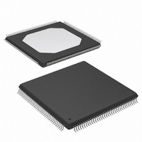
XCS10XL-5TQ144C Xilinx Inc, XCS10XL-5TQ144C Datasheet - Page 5

XCS10XL-5TQ144C
Manufacturer Part Number
XCS10XL-5TQ144C
Description
IC FPGA 3.3V C-TEMP 144-TQFP
Manufacturer
Xilinx Inc
Series
Spartan™-XLr
Datasheet
1.XCS05XL-4VQG100C.pdf
(83 pages)
Specifications of XCS10XL-5TQ144C
Number Of Logic Elements/cells
466
Number Of Labs/clbs
196
Total Ram Bits
6272
Number Of I /o
112
Number Of Gates
10000
Voltage - Supply
3 V ~ 3.6 V
Mounting Type
Surface Mount
Operating Temperature
0°C ~ 85°C
Package / Case
144-LQFP
Case
TQFP144
Dc
02+
Lead Free Status / RoHS Status
Contains lead / RoHS non-compliant
Available stocks
Company
Part Number
Manufacturer
Quantity
Price
Company:
Part Number:
XCS10XL-5TQ144C
Manufacturer:
XILINX
Quantity:
5 530
Company:
Part Number:
XCS10XL-5TQ144C
Manufacturer:
SMD
Quantity:
246
Company:
Part Number:
XCS10XL-5TQ144C
Manufacturer:
XILINX
Quantity:
23
.
Table 2: CLB Storage Element Functionality
DS060 (v1.8) June 26, 2008
Product Specification
Power-Up or
GSR
Flip-Flop
Operation
Latch
Operation
(Spartan-XL)
Both
Figure 3: CLB Flip-Flop Functional Block Diagram
Legend:
Mode
SR
0*
1*
X
CK
EC
D
R
GND
SR
Don’t care
Rising edge (clock not inverted).
Set or Reset value. Reset is default.
Input is Low or unconnected (default
value)
Input is High or unconnected (default
value)
GSR
CK
X
X
X
0
1
0
Vcc
EC
1*
1*
1*
X
X
X
0
Multiplexer Controlled
by Configuration Program
D
SR
SD
RD
0*
0*
0*
0*
0*
X
1
Q
DS060_03_041901
D
X
X
D
X
X
D
X
Q
SR
SR
www.xilinx.com
D
Q
Q
D
Q
Q
Clock Input
Each flip-flop can be triggered on either the rising or falling
clock edge. The CLB clock line is shared by both flip-flops.
However, the clock is individually invertible for each flip-flop
(see CK path in
line in the design is automatically absorbed into the CLB.
Clock Enable
The clock enable line (EC) is active High. The EC line is
shared by both flip-flops in a CLB. If either one is left discon-
nected, the clock enable for that flip-flop defaults to the
active state. EC is not invertible within the CLB. The clock
enable is synchronous to the clock and must satisfy the
setup and hold timing specified for the device.
Set/Reset
The set/reset line (SR) is an asynchronous active High con-
trol of the flip-flop. SR can be configured as either set or
reset at each flip-flop. This configuration option determines
the state in which each flip-flop becomes operational after
configuration. It also determines the effect of a GSR pulse
during normal operation, and the effect of a pulse on the SR
line of the CLB. The SR line is shared by both flip-flops. If
SR is not specified for a flip-flop the set/reset for that flip-flop
defaults to the inactive state. SR is not invertible within the
CLB.
CLB Signal Flow Control
In addition to the H-LUT input control multiplexers (shown in
box "A" of
multiplexers (shown in box "B" of
signals which drive the flip-flop inputs and the combinatorial
CLB outputs (X and Y).
Each flip-flop input is driven from a 4:1 multiplexer which
selects among the three LUT outputs and DIN as the data
source.
Each combinatorial output is driven from a 2:1 multiplexer
which selects between two of the LUT outputs. The X output
can be driven from the F-LUT or H-LUT, the Y output from
G-LUT or H-LUT.
Control Signals
There are four signal control multiplexers on the input of the
CLB. These multiplexers allow the internal CLB control sig-
nals (H1, DIN, SR, and EC in
driven from any of the four general control inputs (C1-C4 in
Figure
the four internal control signals.
Spartan and Spartan-XL FPGA Families Data Sheet
4) into the CLB. Any of these inputs can drive any of
Figure 2, page
Figure
3). Any inverter placed on the clock
4) there are signal flow control
Figure 2
Figure
and
2) which select the
Figure
4) to be
5


