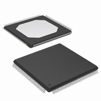
XCS10XL-5TQ144C Xilinx Inc, XCS10XL-5TQ144C Datasheet - Page 14

XCS10XL-5TQ144C
Manufacturer Part Number
XCS10XL-5TQ144C
Description
IC FPGA 3.3V C-TEMP 144-TQFP
Manufacturer
Xilinx Inc
Series
Spartan™-XLr
Datasheet
1.XCS05XL-4VQG100C.pdf
(83 pages)
Specifications of XCS10XL-5TQ144C
Number Of Logic Elements/cells
466
Number Of Labs/clbs
196
Total Ram Bits
6272
Number Of I /o
112
Number Of Gates
10000
Voltage - Supply
3 V ~ 3.6 V
Mounting Type
Surface Mount
Operating Temperature
0°C ~ 85°C
Package / Case
144-LQFP
Case
TQFP144
Dc
02+
Lead Free Status / RoHS Status
Contains lead / RoHS non-compliant
Available stocks
Company
Part Number
Manufacturer
Quantity
Price
Company:
Part Number:
XCS10XL-5TQ144C
Manufacturer:
XILINX
Quantity:
5 530
Company:
Part Number:
XCS10XL-5TQ144C
Manufacturer:
SMD
Quantity:
246
Company:
Part Number:
XCS10XL-5TQ144C
Manufacturer:
XILINX
Quantity:
23
Spartan and Spartan-XL FPGA Families Data Sheet
•
•
•
•
The appropriate choice of RAM configuration mode for a
given design should be based on timing and resource
requirements, desired functionality, and the simplicity of the
design process. Selection criteria include the following:
Whereas the 32 x 1 single-port, the (16 x 1) x 2 single-port,
and the 16 x 1 dual-port configurations each use one entire
CLB, the 16 x 1 single-port configuration uses only one half
of a CLB. Due to its simultaneous read/write capability, the
dual-port RAM can transfer twice as much data as the sin-
gle-port RAM, which permits only one data operation at any
given time.
CLB memory configuration options are selected by using
the appropriate library symbol in the design entry.
Single-Port Mode
There are three CLB memory configurations for the sin-
gle-port RAM: 16 x 1, (16 x 1) x 2, and 32 x 1, the functional
organization of which is shown in
The single-port RAM signals and the CLB signals
page
Table
14
The 16 x 1 single-port configuration contains a RAM
array with 16 locations, each one-bit wide. One 4-bit
address decoder determines the RAM location for write
and read operations. There is one input for writing data
and one output for reading data, all at the selected
address.
The (16 x 1) x 2 single-port configuration combines two
16 x 1 single-port configurations (each according to the
preceding description). There is one data input, one
data output and one address decoder for each array.
These arrays can be addressed independently.
The 32 x 1 single-port configuration contains a RAM
array with 32 locations, each one-bit wide. There is one
data input, one data output, and one 5-bit address
decoder.
The dual-port mode 16 x 1 configuration contains a
RAM array with 16 locations, each one-bit wide. There
are two 4-bit address decoders, one for each port. One
port consists of an input for writing and an output for
reading, all at a selected address. The other port
consists of one output for reading from an
independently selected address.
4) from which they are originally derived are shown in
9.
Figure
12.
(Figure 2,
www.xilinx.com
Table 9: Single-Port RAM Signals
Notes:
1.
2.
Writing data to the single-port RAM is essentially the same
as writing to a data register. It is an edge-triggered (syn-
chronous) operation performed by applying an address to
the A inputs and data to the D input during the active edge
of WCLK while WE is High.
The timing relationships are shown in
logic level on WE enables the input data register for writing.
The active edge of WCLK latches the address, input data,
and WE signals. Then, an internal write pulse is generated
that loads the data into the memory cell.
D0 or D1
A[n-1:0]
WCLK
A4 (32 x 1 only)
Figure 12: Logic Diagram for the Single-Port RAM
WE
RAM Signal
The (16 x 1) x 2 configuration combines two 16 x 1 single-port
RAMs, each with its own independent address bus and data
input. The same WE and WCLK signals are connected to both
RAMs.
n = 4 for the 16 x 1 and (16 x 1) x 2 configurations. n = 5 for the
32 x 1 configuration.
D0 or D1
WCLK
A[3:0]
SPO
WE
n
Single Port Out
Write Enable
(Data Out)
Function
Address
Address
Data In
Clock
CONTROL
WRITE
n
DS060 (v1.8) June 26, 2008
RAM ARRAY
16 x 1
32 x 1
Product Specification
Figure
F[4:1] or G[4:1]
F
READ
CLB Signal
OUT
OUT
DIN or H1
13. The High
SR
H1
or G
K
DS060_12_043010
OUT
SPO
R


