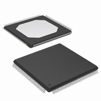
XCS10XL-5TQ144C Xilinx Inc, XCS10XL-5TQ144C Datasheet - Page 59

XCS10XL-5TQ144C
Manufacturer Part Number
XCS10XL-5TQ144C
Description
IC FPGA 3.3V C-TEMP 144-TQFP
Manufacturer
Xilinx Inc
Series
Spartan™-XLr
Datasheet
1.XCS05XL-4VQG100C.pdf
(83 pages)
Specifications of XCS10XL-5TQ144C
Number Of Logic Elements/cells
466
Number Of Labs/clbs
196
Total Ram Bits
6272
Number Of I /o
112
Number Of Gates
10000
Voltage - Supply
3 V ~ 3.6 V
Mounting Type
Surface Mount
Operating Temperature
0°C ~ 85°C
Package / Case
144-LQFP
Case
TQFP144
Dc
02+
Lead Free Status / RoHS Status
Contains lead / RoHS non-compliant
Available stocks
Company
Part Number
Manufacturer
Quantity
Price
Company:
Part Number:
XCS10XL-5TQ144C
Manufacturer:
XILINX
Quantity:
5 530
Company:
Part Number:
XCS10XL-5TQ144C
Manufacturer:
SMD
Quantity:
246
Company:
Part Number:
XCS10XL-5TQ144C
Manufacturer:
XILINX
Quantity:
23
Spartan-XL Family Pin-to-Pin Input Parameter Guidelines
All devices are 100% functionally tested. Pin-to-pin timing
parameters are derived from measuring external and inter-
nal test patterns and are guaranteed over worst-case oper-
Spartan-XL Family Setup and Hold
Capacitive Load Factor
Figure 35
and load capacitance. It allows a user to adjust the specified
output delay if the load capacitance is different than 50 pF.
For example, if the actual load capacitance is 120 pF, add
2.5 ns to the specified delay. If the load capacitance is 20
pF, subtract 0.8 ns from the specified output delay.
Figure 35
of voltage and temperature and is independent of the output
slew rate control.
DS060 (v1.8) June 26, 2008
Product Specification
Notes:
1.
2.
Input Setup/Hold Times Using Global Clock and IFF
T
Symbol
T
IFF = Input Flip-Flop or Latch
Setup time is measured with the fastest route and the lightest load. Hold time is measured using the furthest distance and a
reference load of one clock pin per IOB/CLB.
SUF
SU
/T
/T
HF
H
shows the relationship between I/O output delay
is usable over the specified operating conditions
R
No Delay
Full Delay
Description
www.xilinx.com
ating conditions (supply voltage and junction temperature).
Listed below are representative values for typical pin loca-
tions and normal clock loading.
Figure 35: Delay Factor at Various Capacitive Loads
Spartan and Spartan-XL FPGA Families Data Sheet
-1
-2
3
2
1
0
XCS05XL
XCS10XL
XCS20XL
XCS30XL
XCS40XL
XCS05XL
XCS10XL
XCS20XL
XCS30XL
XCS40XL
0
Device
20
40
1.1/2.0
1.0/2.2
0.9/2.4
0.8/2.6
0.7/2.8
3.9/0.0
4.1/0.0
4.3/0.0
4.5/0.0
4.7/0.0
Capacitance (pF)
Max
-5
Speed Grade
60
80
1.6/2.6
1.5/2.8
1.4/3.0
1.3/3.2
1.2/3.4
5.1/0.0
5.3/0.0
5.5/0.0
5.7/0.0
5.9/0.0
Max
-4
100
DS060_35_080400
120
Units
ns
ns
ns
ns
ns
ns
ns
ns
ns
ns
140
59


