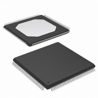
XCS10XL-5TQ144C Xilinx Inc, XCS10XL-5TQ144C Datasheet - Page 9

XCS10XL-5TQ144C
Manufacturer Part Number
XCS10XL-5TQ144C
Description
IC FPGA 3.3V C-TEMP 144-TQFP
Manufacturer
Xilinx Inc
Series
Spartan™-XLr
Datasheet
1.XCS05XL-4VQG100C.pdf
(83 pages)
Specifications of XCS10XL-5TQ144C
Number Of Logic Elements/cells
466
Number Of Labs/clbs
196
Total Ram Bits
6272
Number Of I /o
112
Number Of Gates
10000
Voltage - Supply
3 V ~ 3.6 V
Mounting Type
Surface Mount
Operating Temperature
0°C ~ 85°C
Package / Case
144-LQFP
Case
TQFP144
Dc
02+
Lead Free Status / RoHS Status
Contains lead / RoHS non-compliant
Available stocks
Company
Part Number
Manufacturer
Quantity
Price
Company:
Part Number:
XCS10XL-5TQ144C
Manufacturer:
XILINX
Quantity:
5 530
Company:
Part Number:
XCS10XL-5TQ144C
Manufacturer:
SMD
Quantity:
246
Company:
Part Number:
XCS10XL-5TQ144C
Manufacturer:
XILINX
Quantity:
23
Output Multiplexer/2-Input Function Generator
(Spartan-XL Family Only)
The output path in the Spartan-XL family IOB contains an
additional multiplexer not available in the Spartan family
IOB. The multiplexer can also be configured as a 2-input
function generator, implementing a pass gate, AND gate,
OR gate, or XOR gate, with 0, 1, or 2 inverted inputs.
When configured as a multiplexer, this feature allows two
output signals to time-share the same output pad, effec-
tively doubling the number of device outputs without requir-
ing a larger, more expensive package. The select input is
the pin used for the output flip-flop clock, OK.
When the multiplexer is configured as a 2-input function
generator, logic can be implemented within the IOB itself.
Combined with a Global buffer, this arrangement allows
very high-speed gating of a single signal. For example, a
wide decoder can be implemented in CLBs, and its output
gated with a Read or Write Strobe driven by a global buffer.
The user can specify that the IOB function generator be
used by placing special library symbols beginning with the
letter "O." For example, a 2-input AND gate in the IOB func-
tion generator is called OAND2. Use the symbol input pin
labeled "F" for the signal on the critical path. This signal is
placed on the OK pin — the IOB input with the shortest
delay to the function generator. Two examples are shown in
Figure
Output Buffer
An active High 3-state signal can be used to place the out-
put buffer in a high-impedance state, implementing 3-state
outputs or bidirectional I/O. Under configuration control, the
output (O) and output 3-state (T) signals can be inverted.
The polarity of these signals is independently configured for
each IOB (see
ured as open-drain (open-collector) by tying the 3-state pin
(T) to the output signal, and the input pin (I) to Ground.
DS060 (v1.8) June 26, 2008
Product Specification
Figure 7: AND and MUX Symbols in Spartan-XL IOB
7.
R
OAND2
F
Figure 6, page
7). An output can be config-
D0
D1
S0
OMUX2
DS060_07_081100
O
www.xilinx.com
By default, a 5V Spartan device output buffer pull-up struc-
ture is configured as a TTL-like totem-pole. The High driver
is an n-channel pull-up transistor, pulling to a voltage one
transistor threshold below V
can be globally configured as CMOS drivers, with additional
p-channel pull-up transistors pulling to V
applied using the bitstream generation software, applies to
all outputs on the device. It is not individually programma-
ble.
All Spartan-XL device outputs are configured as CMOS
drivers, therefore driving rail-to-rail. The Spartan-XL family
outputs are individually programmable for 12 mA or 24 mA
output drive.
Any 5V Spartan device with its outputs configured in TTL
mode can drive the inputs of any typical 3.3V device. Sup-
ported destinations for Spartan/XL device outputs are
shown in
Three-State Register (Spartan-XL Family Only)
Spartan-XL devices incorporate an optional register control-
ling the three-state enable in the IOBs. The use of the
three-state control register can significantly improve output
enable and disable time.
Output Slew Rate
The slew rate of each output buffer is, by default, reduced,
to minimize power bus transients when switching non-criti-
cal signals. For critical signals, attach a FAST attribute or
property to the output buffer or flip-flop.
Spartan/XL devices have a feature called "Soft Start-up,"
designed to reduce ground bounce when all outputs are
turned on simultaneously at the end of configuration.
When the configuration process is finished and the device
starts up, the first activation of the outputs is automatically
slew-rate limited. Immediately following the initial activation
of the I/O, the slew rate of the individual outputs is deter-
mined by the individual configuration option for each IOB.
Pull-up and Pull-down Network
Programmable pull-up and pull-down resistors are used for
tying unused pins to V
sumption and reduce noise sensitivity. The configurable
pull-up resistor is a p-channel transistor that pulls to V
The configurable pull-down resistor is an n-channel transis-
tor that pulls to Ground. The value of these resistors is typi-
cally 20 KΩ − 100 KΩ
Characteristics Over Operating Conditions" on page
Spartan and Spartan-XL FPGA Families Data Sheet
Table
7.
CC
or Ground to minimize power con-
(See "Spartan Family DC
CC
. Alternatively, the outputs
CC
. This option,
43.).
CC
9
.


