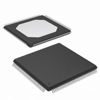
XCS10XL-5TQ144C Xilinx Inc, XCS10XL-5TQ144C Datasheet - Page 28

XCS10XL-5TQ144C
Manufacturer Part Number
XCS10XL-5TQ144C
Description
IC FPGA 3.3V C-TEMP 144-TQFP
Manufacturer
Xilinx Inc
Series
Spartan™-XLr
Datasheet
1.XCS05XL-4VQG100C.pdf
(83 pages)
Specifications of XCS10XL-5TQ144C
Number Of Logic Elements/cells
466
Number Of Labs/clbs
196
Total Ram Bits
6272
Number Of I /o
112
Number Of Gates
10000
Voltage - Supply
3 V ~ 3.6 V
Mounting Type
Surface Mount
Operating Temperature
0°C ~ 85°C
Package / Case
144-LQFP
Case
TQFP144
Dc
02+
Lead Free Status / RoHS Status
Contains lead / RoHS non-compliant
Available stocks
Company
Part Number
Manufacturer
Quantity
Price
Company:
Part Number:
XCS10XL-5TQ144C
Manufacturer:
XILINX
Quantity:
5 530
Company:
Part Number:
XCS10XL-5TQ144C
Manufacturer:
SMD
Quantity:
246
Company:
Part Number:
XCS10XL-5TQ144C
Manufacturer:
XILINX
Quantity:
23
Spartan and Spartan-XL FPGA Families Data Sheet
Slave Serial is the default mode if the Mode pins are left
unconnected, as they have weak pull-up resistors during
configuration.
Multiple slave devices with identical configurations can be
wired with parallel DIN inputs. In this way, multiple devices
can be configured simultaneously.
Serial Daisy Chain
Multiple devices with different configurations can be con-
nected together in a "daisy chain," and a single combined
bitstream used to configure the chain of slave devices.
To configure a daisy chain of devices, wire the CCLK pins of
all devices in parallel, as shown in
DOUT of each device to the DIN of the next. The lead or
master FPGA and following slaves each passes resynchro-
nized configuration data coming from a single source. The
header data, including the length count, is passed through
28
PROGRAM
MODE
DONE
PROGRAM
Spartan
Master
Seria
l
DOUT
CCLK
LDC
INIT
DIN
Figure 25: Master/Slave Serial Mode Circuit Diagram
Figure
V
CC
3.3K
25. Connect the
(Low Reset Option Used)
Xilinx SPROM
CE
RESET/OE
CLK
DATA
www.xilinx.com
CEO
V
PP
+5V
and is captured by each FPGA when it recognizes the 0010
preamble. Following the length-count data, each FPGA out-
puts a High on DOUT until it has received its required num-
ber of data frames.
After an FPGA has received its configuration data, it passes
on any additional frame start bits and configuration data on
DOUT. When the total number of configuration clocks
applied after memory initialization equals the value of the
24-bit length count, the FPGAs begin the start-up sequence
and become operational together. FPGA I/O are normally
released two CCLK cycles after the last configuration bit is
received.
The daisy-chained bitstream is not simply a concatenation
of the individual bitstreams. The PROM File Formatter must
be used to combine the bitstreams for a daisy-chained con-
figuration.
N/C
CCLK
PROGRAM
DONE
DIN
MODE
Spartan
Slave
DOUT
INIT
V
CC
3.3K
DS060 (v1.8) June 26, 2008
3.3K
Note:
M2, M1, M0 can be shorted
to V
D/P
M2
RESET
DIN
CCLK
CC
Product Specification
M0
if not used as I/O
M1
FPGA
Slave
3.3K
DOUT
DS060_25_061301
INIT
R


