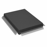
AD9888KSZ-140 Analog Devices Inc, AD9888KSZ-140 Datasheet - Page 10

AD9888KSZ-140
Manufacturer Part Number
AD9888KSZ-140
Description
IC FLAT PANEL INTERFACE 128-MQFP
Manufacturer
Analog Devices Inc
Datasheet
1.AD9888KSZ-205.pdf
(32 pages)
Specifications of AD9888KSZ-140
Applications
Graphic Cards, VGA Interfaces
Interface
2-Wire Serial
Voltage - Supply
3 V ~ 3.6 V
Package / Case
128-MQFP, 128-PQFP
Mounting Type
Surface Mount
Supply Current
200mA
Power Dissipation Pd
850mW
Supply Voltage Range
3V To 3.6V, 2.2V To 3.6V
Digital Ic Case Style
MQFP
No. Of Pins
128
Operating Temperature Range
0°C To +70°C
Svhc
No SVHC
Number Of Elements
3
Resolution
8Bit
Sample Rate
140MSPS
Input Polarity
Bipolar
Input Type
Voltage
Rated Input Volt
±0.25/±0.5V
Differential Input
No
Power Supply Requirement
Single
Single Supply Voltage (typ)
3.3V
Single Supply Voltage (min)
3V
Single Supply Voltage (max)
3.6V
Dual Supply Voltage (typ)
Not RequiredV
Dual Supply Voltage (min)
Not RequiredV
Dual Supply Voltage (max)
Not RequiredV
Power Dissipation
1.05W
Differential Linearity Error
±1.35LSB
Integral Nonlinearity Error
±2.5LSB
Operating Temp Range
0C to 70C
Operating Temperature Classification
Commercial
Mounting
Surface Mount
Pin Count
128
Package Type
MQFP
Input Signal Type
Single-Ended
Interface Type
2-wire, Serial
Rohs Compliant
Yes
Lead Free Status / RoHS Status
Lead free / RoHS Compliant
Lead Free Status / RoHS Status
Lead free / RoHS Compliant, Lead free / RoHS Compliant
Available stocks
Company
Part Number
Manufacturer
Quantity
Price
Company:
Part Number:
AD9888KSZ-140
Manufacturer:
AD
Quantity:
217
Company:
Part Number:
AD9888KSZ-140
Manufacturer:
ADI
Quantity:
482
Company:
Part Number:
AD9888KSZ-140
Manufacturer:
Analog Devices Inc
Quantity:
10 000
AD9888
The offset controls provide a ±63 LSB adjustment range. This
range is connected with the full-scale range, so if the input range
is doubled (from 0.5 V to 1.0 V), the offset step size is also
doubled (from 2 mV per step to 4 mV per step).
Figure 2 illustrates the interaction of gain and offset controls.
The magnitude of an LSB in offset adjustment is proportional
to the full-scale range, so changing the full-scale range also
changes the offset. The change is minimal if the offset setting is
near midscale. When changing the offset, the full-scale range is
not affected, but the full-scale level is shifted by the same amount
as the zero-scale level.
Sync-on-Green
The Sync-on-Green input operates in two steps. First, it sets a
baseline clamp level off of the incoming video signal with a
negative peak detector. Second, it sets the sync trigger level
(nominally 150 mV above the negative peak). The exact trigger
level is variable and can be programmed via Register 11H. The
Sync-on-Green input must be ac-coupled to the green analog input
through its own capacitor, as shown in Figure 3. The value of
the capacitor must be 1 nF ± 20%. If Sync-on-Green is not used,
this connection is not required and the SOGIN pin should be
left unconnected. (Note: the Sync-on-Green signal is always
negative polarity.) For more details, see the Sync Processing section.
Clock Generation
A phase locked loop (PLL) is employed to generate the pixel
clock. The Hsync input provides a reference frequency to the
PLL. A voltage controlled oscillator (VCO) generates a much
higher pixel clock frequency. This pixel clock is divided by the
PLL divide value (Registers 01H and 02H) and phase compared
with the Hsync input. Any error is used to shift the VCO
frequency and maintain lock between the two signals.
1.0
0.5
0.0
Figure 3. Typical Clamp Configuration for
RGB/YUV Applications
00h
Figure 2. Gain and Offset Control
47nF
47nF
47nF
1nF
R
B
G
SOG
GAIN
AIN
AIN
AIN
OFFSET = 7Fh
OFFSET = 3Fh
OFFSET = 00h
OFFSET = 7Fh
OFFSET = 3Fh
OFFSET = 00h
FFh
–10–
The stability of this clock is a very important element in providing
the clearest and most stable image. During each pixel time,
there is a period during which the signal is slewing from the old
pixel amplitude and settling at its new value. Then there is a
time when the input voltage is stable, before the signal must
slew to a new value (Figure 4). The ratio of the slewing time to
the stable time is a function of the bandwidth of the graphics
DAC and the bandwidth of the transmission system (cable and
termination). It is also a function of the overall pixel rate.
Clearly, if the dynamic characteristics of the system remain
fixed, then the slewing and settling time is likewise fixed. This
time must be subtracted from the total pixel period, leaving the
stable period. At higher pixel frequencies, the total cycle time is
shorter and the stable pixel time becomes shorter as well.
Any jitter in the clock reduces the precision with which the
sampling time can be determined, and must also be subtracted
from the stable pixel time.
Considerable care has been taken in the design of the AD9888’s
clock generation circuit to minimize jitter. As indicated in
Figure 5, the clock jitter of the AD9888 is less than 9% of the
total pixel time in all operating modes, making the reduction in
the valid sampling time due to jitter negligible.
The PLL characteristics are determined by the loop filter design,
the PLL charge pump current, and the VCO range setting. The
loop filter design is illustrated in Figure 6. Recommended settings
of VCO range and charge pump current for VESA standard
display modes are listed in Table IV.
14
12
10
Figure 5. Pixel Clock Jitter vs. Frequency
8
6
4
2
0
PIXEL CLOCK
Figure 4. Pixel Sampling Times
INVALID SAMPLE
PIXEL CLOCK – MHz
TIMES
REV. B


