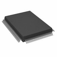
AD9888KSZ-140 Analog Devices Inc, AD9888KSZ-140 Datasheet - Page 24

AD9888KSZ-140
Manufacturer Part Number
AD9888KSZ-140
Description
IC FLAT PANEL INTERFACE 128-MQFP
Manufacturer
Analog Devices Inc
Datasheet
1.AD9888KSZ-205.pdf
(32 pages)
Specifications of AD9888KSZ-140
Applications
Graphic Cards, VGA Interfaces
Interface
2-Wire Serial
Voltage - Supply
3 V ~ 3.6 V
Package / Case
128-MQFP, 128-PQFP
Mounting Type
Surface Mount
Supply Current
200mA
Power Dissipation Pd
850mW
Supply Voltage Range
3V To 3.6V, 2.2V To 3.6V
Digital Ic Case Style
MQFP
No. Of Pins
128
Operating Temperature Range
0°C To +70°C
Svhc
No SVHC
Number Of Elements
3
Resolution
8Bit
Sample Rate
140MSPS
Input Polarity
Bipolar
Input Type
Voltage
Rated Input Volt
±0.25/±0.5V
Differential Input
No
Power Supply Requirement
Single
Single Supply Voltage (typ)
3.3V
Single Supply Voltage (min)
3V
Single Supply Voltage (max)
3.6V
Dual Supply Voltage (typ)
Not RequiredV
Dual Supply Voltage (min)
Not RequiredV
Dual Supply Voltage (max)
Not RequiredV
Power Dissipation
1.05W
Differential Linearity Error
±1.35LSB
Integral Nonlinearity Error
±2.5LSB
Operating Temp Range
0C to 70C
Operating Temperature Classification
Commercial
Mounting
Surface Mount
Pin Count
128
Package Type
MQFP
Input Signal Type
Single-Ended
Interface Type
2-wire, Serial
Rohs Compliant
Yes
Lead Free Status / RoHS Status
Lead free / RoHS Compliant
Lead Free Status / RoHS Status
Lead free / RoHS Compliant, Lead free / RoHS Compliant
Available stocks
Company
Part Number
Manufacturer
Quantity
Price
Company:
Part Number:
AD9888KSZ-140
Manufacturer:
AD
Quantity:
217
Company:
Part Number:
AD9888KSZ-140
Manufacturer:
ADI
Quantity:
482
Company:
Part Number:
AD9888KSZ-140
Manufacturer:
Analog Devices Inc
Quantity:
10 000
AD9888
14
14
14
14
HSYNC Polarity Status
0
1
Bit 7
(Hsync
Detect)
0
0
1
1
X
Table XXVII. Detected Hsync Input Polarity Status
7
This bit is used to indicate when activity is detected on
the selected Hsync input pin. If HSYNC is held high or
low, activity will not be detected.
The sync processing block diagram shows where this
function is implemented.
6
This bit indicates which Hsync input source is being used
by the PLL (Hsync input or Sync-on-Green). Bits 7 and 1
in this register are what determine which source is used. If
both Hsync and SOG are detected, the user can determine
which has priority via Bit 3 in register 0EH. The user can
override this function via Bit 4 in Register 0EH. If the
override bit is set to Logic 1, then this bit will be forced
to whatever the state of Bit 3 in Register 0EH is set to.
AHS = 0 means use the HSYNC pin input for HSYNC.
AHS = 1 means use the SOG pin input for HSYNC.
The override bit is in Register 0EH, Bit 4.
5
This bit reports the status of the HSYNC input polarity
detection circuit. It can be used to determine the polarity
of the HSYNC input. The detection circuit’s location is
shown in the Sync Processing Block Diagram (Figure 25).
4
This bit is used to indicate when activity is detected on
the selected Vsync input pin. If Vsync is held high or low,
activity will not be detected.
Table XXVIII. Vsync Detection Results
Hsync Detect
AHS – Active Hsync
Detected Hsync Input Polarity Status
Vsync Detect
Table XXV. Hsync Detection Results
Detect
0
1
Table XXVI. Active Hsync Results
Detect
0
1
Bit 1
(SOG
Detect)
0
1
0
1
X
Function
No Activity Detected
Activity Detected
Function
No Activity Detected
Activity Detected
Bit 4, Reg
OEH
(Override)
0
0
0
0
1
Result
Hsync Polarity is Negative.
Hsync Polarity is Positive.
AHS
Bit 3 in 0Eh
1
0
Bit 3 in 0Eh
Bit 3 in 0Eh
–24–
14
14
14
14
HSYNC Polarity Status
0
1
Vsync Polarity Status
0
1
Table XXXII. Detected COAST Input Polarity Status
The sync processing block diagram (Figure 25) shows
where this function is implemented.
3
This bit indicates which Vsync source is being used; the
Vsync input or the output from the sync separator. Bit 4
in this register is what determines which is active. If both
Vsync and SOG are detected, the user can determine which
has priority via Bit 0 in Register 0EH. The user can override
this function via Bit 1 in Register 0EH. If the override bit
is set to Logic 1, this bit will be forced to whatever the
state of Bit 0 in Register 0EH is set to.
Bit 5 (Vsync Detect)
0
1
X
AVS = 1 means Sync separator.
AVS = 0 means Vsync input.
The override bit is in register 0Eh, Bit 1.
2
This bit reports the status of the Vsync output polarity
detection circuit. It can be used to determine the polarity
of the Vsync input. The detection circuit’s location is
shown in the sync processing block diagram (Figure 25).
1
This bit is used to indicate when Sync activity is detected
on the selected Sync-on-Green input pin.
The Sync Processing Block Diagram (Figure 25) shows
where this function is implemented.
0
This bit reports the status of the coast input polarity
detection circuit. It can be used to determine the polarity
of the COAST input. The detection circuit’s location is
shown in Figure 25.
Table XXX. Detected Vsync Input Polarity Status
Table XXXI. Sync-on-Green Detection Results
AVS – Active Vsync
Detected Vsync Output Polarity Status
Sync-on-Green Detect
Detected COAST Polarity Status
Table XXIX. Active Vsync Results
Detect
0
1
Function
No Activity Detected
Activity Detected
Result
Vsync Polarity is Active High.
Vsync Polarity is Active Low.
0
0
1
Override
COAST Polarity is Negative.
COAST Polarity is Positive.
Result
AVS
1
0
Bit 0 in 0EH
REV. B


