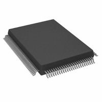
AD9888KSZ-140 Analog Devices Inc, AD9888KSZ-140 Datasheet - Page 3

AD9888KSZ-140
Manufacturer Part Number
AD9888KSZ-140
Description
IC FLAT PANEL INTERFACE 128-MQFP
Manufacturer
Analog Devices Inc
Datasheet
1.AD9888KSZ-205.pdf
(32 pages)
Specifications of AD9888KSZ-140
Applications
Graphic Cards, VGA Interfaces
Interface
2-Wire Serial
Voltage - Supply
3 V ~ 3.6 V
Package / Case
128-MQFP, 128-PQFP
Mounting Type
Surface Mount
Supply Current
200mA
Power Dissipation Pd
850mW
Supply Voltage Range
3V To 3.6V, 2.2V To 3.6V
Digital Ic Case Style
MQFP
No. Of Pins
128
Operating Temperature Range
0°C To +70°C
Svhc
No SVHC
Number Of Elements
3
Resolution
8Bit
Sample Rate
140MSPS
Input Polarity
Bipolar
Input Type
Voltage
Rated Input Volt
±0.25/±0.5V
Differential Input
No
Power Supply Requirement
Single
Single Supply Voltage (typ)
3.3V
Single Supply Voltage (min)
3V
Single Supply Voltage (max)
3.6V
Dual Supply Voltage (typ)
Not RequiredV
Dual Supply Voltage (min)
Not RequiredV
Dual Supply Voltage (max)
Not RequiredV
Power Dissipation
1.05W
Differential Linearity Error
±1.35LSB
Integral Nonlinearity Error
±2.5LSB
Operating Temp Range
0C to 70C
Operating Temperature Classification
Commercial
Mounting
Surface Mount
Pin Count
128
Package Type
MQFP
Input Signal Type
Single-Ended
Interface Type
2-wire, Serial
Rohs Compliant
Yes
Lead Free Status / RoHS Status
Lead free / RoHS Compliant
Lead Free Status / RoHS Status
Lead free / RoHS Compliant, Lead free / RoHS Compliant
Available stocks
Company
Part Number
Manufacturer
Quantity
Price
Company:
Part Number:
AD9888KSZ-140
Manufacturer:
AD
Quantity:
217
Company:
Part Number:
AD9888KSZ-140
Manufacturer:
ADI
Quantity:
482
Company:
Part Number:
AD9888KSZ-140
Manufacturer:
Analog Devices Inc
Quantity:
10 000
Parameter
DYNAMIC PERFORMANCE
THERMAL CHARACTERISTICS
NOTES
1
2
3
4
5
6
7
Specifications subject to change without notice.
ABSOLUTE MAXIMUM RATINGS*
V
V
Analog Inputs . . . . . . . . . . . . . . . . . . . . . . . . . . . . V
VREF IN . . . . . . . . . . . . . . . . . . . . . . . . . . . . . . . . V
Digital Inputs . . . . . . . . . . . . . . . . . . . . . . . . . . . 5 V to 0.0 V
Digital Output Current . . . . . . . . . . . . . . . . . . . . . . . . . 20 mA
Operating Temperature . . . . . . . . . . . . . . . . . –25°C to +85°C
Storage Temperature . . . . . . . . . . . . . . . . . . –65°C to +150°C
Maximum Junction Temperature . . . . . . . . . . . . . . . . . 150°C
Maximum Case Temperature . . . . . . . . . . . . . . . . . . . . 150°C
*Stresses above those listed under Absolute Maximum Ratings may cause permanent
CAUTION
ESD (electrostatic discharge) sensitive device. Electrostatic charges as high as 4000 V readily
accumulate on the human body and test equipment and can discharge without detection. Although the
AD9888 features proprietary ESD protection circuitry, permanent damage may occur on devices
subjected to high energy electrostatic discharges. Therefore, proper ESD precautions are recommended
to avoid performance degradation or loss of functionality.
REV. B
AD9888KS-100 specifications are tested at 100 MHz. AD9888KS-140 specifications are tested at 140 MHz.
See Figure 23.
VCO Range = 10, Charge Pump Current = 100, PLL Divider = 1693.
VCO Range = 11, Charge Pump Current = 100, PLL Divider = 2159.
DEMUX = 1, DATACK and DATACK Load = 15 pF, Data Load = 5 pF.
Maximum bandwidth setting. Bandwidth can also be programmed to 300 MHz, 150 MHz, and 75 MHz.
Using External Pixel Clock.
damage to the device. This is a stress rating only; functional operation of the device
at these or any other conditions outside of those indicated in the operation sections
of this specification is not implied. Exposure to absolute maximum ratings for
extended periods may affect device reliability.
D
DD
Analog Bandwidth, Full Power
Transient Response
Overvoltage Recovery Time
Signal-to-Noise Ratio (SNR)
Crosstalk
JC
JA
(Without Harmonics)
f
Thermal Resistance
Thermal Resistance
IN
. . . . . . . . . . . . . . . . . . . . . . . . . . . . . . . . . . . . . . . . . . 3.6 V
—Junction-to-Case
—Junction-to-Ambient
. . . . . . . . . . . . . . . . . . . . . . . . . . . . . . . . . . . . . . . . . 3.6 V
= 40.7 MHz
7
6
Temp Level Min
25°C
25°C
25°C
25°C
Full
Full
Model
AD9888KS-100
AD9888KS-140
AD9888KS-170
AD9888KS-205
AD9888/PCB
Test
V
V
V
IV
V
V
V
V
42
AD9888KS-100/-140
500
2
1.5
45
44
50
35
Typ
8.4
D
D
Temperature Range
0ºC to +70ºC
0ºC to +70ºC
0ºC to +70ºC
0ºC to +70ºC
25ºC
ORDERING GUIDE
to 0.0 V
to 0.0 V
Max
–3–
1
EXPLANATION OF TEST LEVELS
Test Level
I.
II. 100% production tested at 25°C and sample tested at
III. Sample tested only.
IV. Parameter is guaranteed by design and characterization
V. Parameter is a typical value only.
VI. 100% production tested at 25°C; guaranteed by design and
Min
41
100% production tested.
specified temperatures.
testing.
characterization testing.
AD9888KS-170
Typ
500
2
1.5
44
43
50
8.4
35
Package Option
S-128A
S-128A
S-128A
S-128A
Evaluation Board
Max
Min
40
AD9888KS-205
Typ
500
2
1.5
42
41
50
8.4
35
Max
AD9888
Unit
MHz
ns
ns
dB
dB
dBc
°C/W
°C/W


