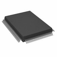
AD9888KSZ-140 Analog Devices Inc, AD9888KSZ-140 Datasheet - Page 13

AD9888KSZ-140
Manufacturer Part Number
AD9888KSZ-140
Description
IC FLAT PANEL INTERFACE 128-MQFP
Manufacturer
Analog Devices Inc
Datasheet
1.AD9888KSZ-205.pdf
(32 pages)
Specifications of AD9888KSZ-140
Applications
Graphic Cards, VGA Interfaces
Interface
2-Wire Serial
Voltage - Supply
3 V ~ 3.6 V
Package / Case
128-MQFP, 128-PQFP
Mounting Type
Surface Mount
Supply Current
200mA
Power Dissipation Pd
850mW
Supply Voltage Range
3V To 3.6V, 2.2V To 3.6V
Digital Ic Case Style
MQFP
No. Of Pins
128
Operating Temperature Range
0°C To +70°C
Svhc
No SVHC
Number Of Elements
3
Resolution
8Bit
Sample Rate
140MSPS
Input Polarity
Bipolar
Input Type
Voltage
Rated Input Volt
±0.25/±0.5V
Differential Input
No
Power Supply Requirement
Single
Single Supply Voltage (typ)
3.3V
Single Supply Voltage (min)
3V
Single Supply Voltage (max)
3.6V
Dual Supply Voltage (typ)
Not RequiredV
Dual Supply Voltage (min)
Not RequiredV
Dual Supply Voltage (max)
Not RequiredV
Power Dissipation
1.05W
Differential Linearity Error
±1.35LSB
Integral Nonlinearity Error
±2.5LSB
Operating Temp Range
0C to 70C
Operating Temperature Classification
Commercial
Mounting
Surface Mount
Pin Count
128
Package Type
MQFP
Input Signal Type
Single-Ended
Interface Type
2-wire, Serial
Rohs Compliant
Yes
Lead Free Status / RoHS Status
Lead free / RoHS Compliant
Lead Free Status / RoHS Status
Lead free / RoHS Compliant, Lead free / RoHS Compliant
Available stocks
Company
Part Number
Manufacturer
Quantity
Price
Company:
Part Number:
AD9888KSZ-140
Manufacturer:
AD
Quantity:
217
Company:
Part Number:
AD9888KSZ-140
Manufacturer:
ADI
Quantity:
482
Company:
Part Number:
AD9888KSZ-140
Manufacturer:
Analog Devices Inc
Quantity:
10 000
TIMING
The following timing diagrams show the operation of the AD9888
analog interface in all clock modes. The part establishes timing
by sending the sample that corresponds to the pixel digitized
when the leading edge of Hsync occurs sent to the “A” data port.
In dual-channel mode, the next sample is to the “B” port. Future
samples are alternated between the “A” and “B” data ports. In
single-channel mode, data is only sent to the “A” data port, and
the “B” port is placed in a high impedance state.
The Output Data Clock signal is created so that its rising edge
always occurs between “A” data transitions, and can be used to
latch the output data externally.
Hsync Timing
Horizontal sync is processed in the AD9888 to eliminate
ambiguity in the timing of the leading edge with respect to the
phase-delayed pixel clock and data.
REV. B
DATACK
DATACK
HSOUT
DATA
Figure 12. Output Timing
t
DCYCLE
t
SKEW
t
PER
–13–
The Hsync input is used as a reference to generate the pixel
sampling clock. The sampling phase can be adjusted, with respect
to Hsync, through a full 360° in 32 steps via the Phase Adjust
Register (to optimize the pixel sampling time). Display systems
use Hsync to align memory and display write cycles, so it is
important to have a stable timing relationship between Hsync
output (HSOUT) and data clock (DATACK).
Three things happen to Horizontal Sync in the AD9888. First,
the polarity of Hsync input is determined and will thus have a
known output polarity. The known output polarity can be pro-
grammed either active high or active low (Register 0EH, Bit 5).
Second, HSOUT is aligned with DATACK and data outputs.
Third, the duration of HSOUT (in pixel clocks) is set via
Register 07H. HSOUT is the sync signal that should be used to
drive the rest of the display system.
COAST Timing
In most computer systems, the Hsync signal is provided con-
tinuously on a dedicated wire. In these systems, the COAST
input and function are unnecessary, and should not be used.
In some systems, however, Hsync is disturbed during the Verti-
cal Sync period (Vsync). In some cases, Hsync pulses disappear.
In other systems, such as those that employ Composite Sync
(Csync) signals or embedded Sync-On-Green (SOG), Hsync
includes equalization pulses or other distortions during Vsync.
To avoid upsetting the clock generator during Vsync, it is impor-
tant to ignore these distortions. If the pixel clock PLL sees
extraneous pulses, it will attempt to lock to this new frequency,
and will have changed frequency by the end of the Vsync period.
It will then take a few lines of correct Hsync timing to recover at
the beginning of a new frame, resulting in a “tearing” of the
image at the top of the display.
The COAST input is provided to eliminate this problem. It is
an asynchronous input that disables the PLL input and allows
the clock to free-run at its then-current frequency. The PLL can
free-run for several lines without significant frequency drift.
AD9888


