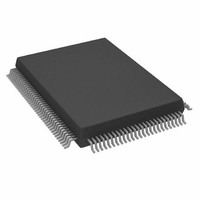
AD9888KSZ-140 Analog Devices Inc, AD9888KSZ-140 Datasheet - Page 17

AD9888KSZ-140
Manufacturer Part Number
AD9888KSZ-140
Description
IC FLAT PANEL INTERFACE 128-MQFP
Manufacturer
Analog Devices Inc
Datasheet
1.AD9888KSZ-205.pdf
(32 pages)
Specifications of AD9888KSZ-140
Applications
Graphic Cards, VGA Interfaces
Interface
2-Wire Serial
Voltage - Supply
3 V ~ 3.6 V
Package / Case
128-MQFP, 128-PQFP
Mounting Type
Surface Mount
Supply Current
200mA
Power Dissipation Pd
850mW
Supply Voltage Range
3V To 3.6V, 2.2V To 3.6V
Digital Ic Case Style
MQFP
No. Of Pins
128
Operating Temperature Range
0°C To +70°C
Svhc
No SVHC
Number Of Elements
3
Resolution
8Bit
Sample Rate
140MSPS
Input Polarity
Bipolar
Input Type
Voltage
Rated Input Volt
±0.25/±0.5V
Differential Input
No
Power Supply Requirement
Single
Single Supply Voltage (typ)
3.3V
Single Supply Voltage (min)
3V
Single Supply Voltage (max)
3.6V
Dual Supply Voltage (typ)
Not RequiredV
Dual Supply Voltage (min)
Not RequiredV
Dual Supply Voltage (max)
Not RequiredV
Power Dissipation
1.05W
Differential Linearity Error
±1.35LSB
Integral Nonlinearity Error
±2.5LSB
Operating Temp Range
0C to 70C
Operating Temperature Classification
Commercial
Mounting
Surface Mount
Pin Count
128
Package Type
MQFP
Input Signal Type
Single-Ended
Interface Type
2-wire, Serial
Rohs Compliant
Yes
Lead Free Status / RoHS Status
Lead free / RoHS Compliant
Lead Free Status / RoHS Status
Lead free / RoHS Compliant, Lead free / RoHS Compliant
Available stocks
Company
Part Number
Manufacturer
Quantity
Price
Company:
Part Number:
AD9888KSZ-140
Manufacturer:
AD
Quantity:
217
Company:
Part Number:
AD9888KSZ-140
Manufacturer:
ADI
Quantity:
482
Company:
Part Number:
AD9888KSZ-140
Manufacturer:
Analog Devices Inc
Quantity:
10 000
2-WIRE SERIAL REGISTER MAP
The AD9888 is initialized and controlled by a set of registers that determine the operating modes. An external controller is employed
to write and read the Control Registers through the 2-line serial interface port.
Hex
Address Read Only Bits Value
00H
01H
02H
03H
04H
05H
06H
07H
08H
09H
0AH
0BH
0CH
0DH
REV. B
Read and
Write or
RO
R/W
R/W
R/W
R/W
R/W
R/W
R/W
R/W
R/W
R/W
R/W
R/W
R/W
DATACK
ADCCK
GOUTA
ROUTA
HSYNC
HSOUT
RGBIN
PXCK
HS
7:0
7:0
7:4
7:2
7:3
7:0
7:0
7:0
7:0
7:0
7:0
7:1
7:1
7:1
P0
Default
01101001 PLL Div MSB
1101**** PLL Div LSB
01****** VCO/CPMP
**001***
10000*** Phase Adjust
00001000 Clamp Placement Places the Clamp signal an integer number of clock periods after the
00010100 Clamp Duration Number of clock periods that the Clamp signal is actively clamping.
00100000 Hsync Output
10000000 Red Gain
10000000 Green Gain
10000000 Blue Gain
1000000* Red Offset
1000000* Green Offset
1000000* Blue Offset
P1
8 PIPE DELAY
P2
Register Name Function
Chip Revision
Pulsewidth
P3
P4
Figure 22. 4:2:2 Output Mode
Table V. Control Register Map
P5
P6
An 8-bit register that represents the silicon revision level.
Sets the number of pixel clocks that HSOUT will remain active.
Controls ADC input range (contrast) of each respective channel. Big
Revision 0 = 0000 0000.
This register is for Bits [11:4] of the PLL divider. Larger values mean the
PLL operates at a faster rate. This register should be loaded first whenever
a change is needed. (This will give the PLL more time to lock.)*
Bits [7:4] LSBs of the PLL divider word.*
Bits [7:6] VCO Range. Selects VCO frequency range. (See PLL description.)
Bits [5:3] Charge Pump Current. Varies the current that drives the low-
pass filter. (See PLL description.)
ADC Clock phase adjustment. Larger values mean more delay.
(1 LSB = T/32)
trailing edge of the Hsync signal.
ger values give less contrast.
Controls dc offset (brightness) of each respective channel. Bigger values
decrease brightness.
–17–
P7
Y0
U0
VARIABLE DURATION
Y1
V0
U2
Y2
Y3
V2
Y4
U4
Y5
V4
AD9888


