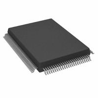
AD9888KSZ-140 Analog Devices Inc, AD9888KSZ-140 Datasheet - Page 25

AD9888KSZ-140
Manufacturer Part Number
AD9888KSZ-140
Description
IC FLAT PANEL INTERFACE 128-MQFP
Manufacturer
Analog Devices Inc
Datasheet
1.AD9888KSZ-205.pdf
(32 pages)
Specifications of AD9888KSZ-140
Applications
Graphic Cards, VGA Interfaces
Interface
2-Wire Serial
Voltage - Supply
3 V ~ 3.6 V
Package / Case
128-MQFP, 128-PQFP
Mounting Type
Surface Mount
Supply Current
200mA
Power Dissipation Pd
850mW
Supply Voltage Range
3V To 3.6V, 2.2V To 3.6V
Digital Ic Case Style
MQFP
No. Of Pins
128
Operating Temperature Range
0°C To +70°C
Svhc
No SVHC
Number Of Elements
3
Resolution
8Bit
Sample Rate
140MSPS
Input Polarity
Bipolar
Input Type
Voltage
Rated Input Volt
±0.25/±0.5V
Differential Input
No
Power Supply Requirement
Single
Single Supply Voltage (typ)
3.3V
Single Supply Voltage (min)
3V
Single Supply Voltage (max)
3.6V
Dual Supply Voltage (typ)
Not RequiredV
Dual Supply Voltage (min)
Not RequiredV
Dual Supply Voltage (max)
Not RequiredV
Power Dissipation
1.05W
Differential Linearity Error
±1.35LSB
Integral Nonlinearity Error
±2.5LSB
Operating Temp Range
0C to 70C
Operating Temperature Classification
Commercial
Mounting
Surface Mount
Pin Count
128
Package Type
MQFP
Input Signal Type
Single-Ended
Interface Type
2-wire, Serial
Rohs Compliant
Yes
Lead Free Status / RoHS Status
Lead free / RoHS Compliant
Lead Free Status / RoHS Status
Lead free / RoHS Compliant, Lead free / RoHS Compliant
Available stocks
Company
Part Number
Manufacturer
Quantity
Price
Company:
Part Number:
AD9888KSZ-140
Manufacturer:
AD
Quantity:
217
Company:
Part Number:
AD9888KSZ-140
Manufacturer:
ADI
Quantity:
482
Company:
Part Number:
AD9888KSZ-140
Manufacturer:
Analog Devices Inc
Quantity:
10 000
MODE CONTROL 1
15
15
15
15
REV. B
PARALLEL
0
1
DEMUX
0
1
7
A bit that determines whether all pixels are presented to a
single port (A), or alternating pixels are demultiplexed to
Ports A and B.
When DEMUX = 0, Port B outputs are in a high
impedance state. The maximum data rate for single-port
mode is 110 MHz. The timing diagrams starting with
Figure 13 show the effects of this option.
The power-up default value is 1.
6
A bit that determines whether all pixels are presented to
Port A and Port B simultaneously on every second
DATACK rising edge, or alternately on Port A and
Port B on successive DATACK rising edges.
When in single port mode (DEMUX = 0), this bit is
ignored. The timing diagrams (Figure 17) show the effects
of this option.
The power-up default value is PARALLEL = 1.
5
One bit that determines whether even pixels or odd pixels
go to Port A.
In normal operation (OUTPHASE = 0) when operating
in dual-port output mode (DEMUX = 1), the first sample
after the Hsync leading edge is presented at Port A. Every
subsequent ODD sample appears at Port A. All EVEN
samples go to Port B.
When OUTPHASE = 1, these ports are reversed and the
first sample goes to Port B.
When DEMUX = 0, this bit is ignored as data always
comes out of only Port A.
4
A bit that configures the output data in 4:2:2 mode. This
mode can be used to reduce the number of data lines used
Table XXXV. Output Port Phase Settings
OUTPHASE
0
1
Channel Mode
Table XXXIII. Channel Mode Settings
Output Mode
Output Port Phase
4:2:2 Output Mode Select
Table XXXIV. Output Mode Settings
Function
All data goes to Port A.
Alternate pixels go to Port A and Port B.
Function
Data is interleaved.
Data is simultaneous on every other
data clock.
First Pixel after Hsync
Port A
Port B
–25–
15
15
15
Channel
Red
Green
Blue
from 24 down to 16 for applications using YUV, YCbCr,
or YPbPr graphics signals. A timing diagram for this mode
is shown in Figure 12. Recommended input and output
configurations are shown in Table XXXVII. In 4:2:2
mode, the red and blue channels can be interchanged to
help satisfy board layout or timing requirements, but the
green channel must be configured for Y.
3
A bit that selects either analog inputs from Channel 0 or
the analog inputs from Channel 1.
2-1
Two bits that select the analog bandwidth.
0
A bit that determines the source of the pixel clock.
A Logic 0 enables the internal PLL that generates the
pixel clock from an externally provided HSYNC.
A Logic 1 enables the external CKEXT input pin. In this
mode, the PLL Divide Ratio (PLLDIV) is ignored. The
clock phase adjust (PHASE) is still functional.
The power-up default value is EXTCLK = 0.
Table XXXVII. 4:2:2 Input/Output Configuration
EXTCLK
0
1
Table XXXIX. Analog Bandwidth Control
Table XL. External Clock Select Settings
Table XXXVI. 4:2:2 Output Mode Select
Input Mux Control
Analog Bandwidth Control
External Clock Select
Table XXXVIII. Input Mux Control
Bit 2
1
1
0
0
Control
0
1
Select
0
1
Input Connection
V
Y
U
Bit 1
1
0
1
0
Function
Internally Generated Clock
Externally Provided Clock Signal
Channel Selected
Channel 0
Channel 1
Analog Bandwidth
500 MHz
300 MHz
150 MHz
75 MHz
Output Mode
4:4:4
4:2:2
High Impedance
Output Format
U/V
Y
AD9888


