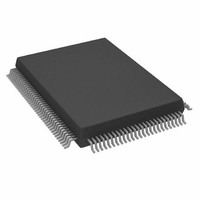
AD9888KSZ-140 Analog Devices Inc, AD9888KSZ-140 Datasheet - Page 28

AD9888KSZ-140
Manufacturer Part Number
AD9888KSZ-140
Description
IC FLAT PANEL INTERFACE 128-MQFP
Manufacturer
Analog Devices Inc
Datasheet
1.AD9888KSZ-205.pdf
(32 pages)
Specifications of AD9888KSZ-140
Applications
Graphic Cards, VGA Interfaces
Interface
2-Wire Serial
Voltage - Supply
3 V ~ 3.6 V
Package / Case
128-MQFP, 128-PQFP
Mounting Type
Surface Mount
Supply Current
200mA
Power Dissipation Pd
850mW
Supply Voltage Range
3V To 3.6V, 2.2V To 3.6V
Digital Ic Case Style
MQFP
No. Of Pins
128
Operating Temperature Range
0°C To +70°C
Svhc
No SVHC
Number Of Elements
3
Resolution
8Bit
Sample Rate
140MSPS
Input Polarity
Bipolar
Input Type
Voltage
Rated Input Volt
±0.25/±0.5V
Differential Input
No
Power Supply Requirement
Single
Single Supply Voltage (typ)
3.3V
Single Supply Voltage (min)
3V
Single Supply Voltage (max)
3.6V
Dual Supply Voltage (typ)
Not RequiredV
Dual Supply Voltage (min)
Not RequiredV
Dual Supply Voltage (max)
Not RequiredV
Power Dissipation
1.05W
Differential Linearity Error
±1.35LSB
Integral Nonlinearity Error
±2.5LSB
Operating Temp Range
0C to 70C
Operating Temperature Classification
Commercial
Mounting
Surface Mount
Pin Count
128
Package Type
MQFP
Input Signal Type
Single-Ended
Interface Type
2-wire, Serial
Rohs Compliant
Yes
Lead Free Status / RoHS Status
Lead free / RoHS Compliant
Lead Free Status / RoHS Status
Lead free / RoHS Compliant, Lead free / RoHS Compliant
Available stocks
Company
Part Number
Manufacturer
Quantity
Price
Company:
Part Number:
AD9888KSZ-140
Manufacturer:
AD
Quantity:
217
Company:
Part Number:
AD9888KSZ-140
Manufacturer:
ADI
Quantity:
482
Company:
Part Number:
AD9888KSZ-140
Manufacturer:
Analog Devices Inc
Quantity:
10 000
AD9888
The AD9888 can digitize graphics signals over a very wide
range of frequencies (10 MHz to 205 MHz). Often, character-
istics that are beneficial at one frequency can be detrimental at
another. Analog bandwidth is one such characteristic. For UXGA
resolutions (up to 205 MHz), a very high analog bandwidth is
desirable because of the fast input signal slew rates. For VGA
and lower resolutions (down to 12.5 MHz), a very high band-
width is not desirable because it allows excess noise to pass
through. To accommodate these varying needs, the AD9888
includes variable analog bandwidth control. Four settings are
available (75 MHz, 150 MHz, 300 MHz, and 500 MHz),
allowing the analog bandwidth to be matched with the resolu-
tion of the incoming graphics signal.
Power Supply Bypassing
It is recommended to bypass each power supply pin with a 0.1 µF
capacitor. The exception is in the case where two or more supply
pins are adjacent to each other. For these groupings of powers/
grounds, it is only necessary to have one bypass capacitor. The
fundamental idea is to have a bypass capacitor within about
0.5 cm of each power pin. Also, avoid placing the capacitor on
VSYNC0
VSYNC1
SOGIN0
SOGIN1
SDA
HSYNC0
HSYNC1
COAST
SCL
MUX5
MUX5
MUX5
BIT 7
ACTIVITY
NEGATIVE PEAK
DETECT
ACTIVITY
CLAMP
DETECT
BIT 6
SYNC SLICER
Figure 24. Serial Interface—Typical Byte Transfer
POLARITY
DETECT
Figure 25. Sync Processing Block Diagram
BIT 5
PLL
MUX4
BIT 4
COMP
SYNC
MUX2
MUX3
–28–
ACTIVITY
DETECT
BIT 3
the opposite side of the PC board from the AD9888, as that
interposes resistive vias in the path.
The bypass capacitors should be physically located between the
power plane and the power pin. Current should flow from the
power plane => capacitor => power pin. Do not make the power
connection between the capacitor and the power pin. Placing a
via underneath the capacitor pads, down to the power plane, is
generally the best approach.
It is particularly important to maintain low noise and good
stability of PV
PV
phase and frequency. This can be avoided by careful attention
to regulation, filtering, and bypassing. It is highly desirable to
provide separate regulated supplies for each of the analog cir-
cuitry groups (V
Some graphic controllers use substantially different levels of
power when active (during active picture time) and when idle
(during horizontal and vertical sync periods). This can result in
a measurable change in the voltage supplied to the analog supply
regulator, which can in turn produce changes in the regulated
D
POLARITY
POLARITY
DETECT
DETECT
can result in similarly abrupt changes in sampling clock
MUX1
BIT 2
D
GENERATOR
(the clock generator supply). Abrupt changes in
D
CLOCK
and PV
BIT 1
SYNC SEPARATOR
INTEGRATOR
D
).
1/S
BIT 0
PIXEL CLOCK
VSYNC
ACK
HSYNCOUT
VSYNCOUT
SOGOUT
REV. B


