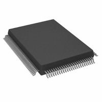
AD9888KSZ-140 Analog Devices Inc, AD9888KSZ-140 Datasheet - Page 22

AD9888KSZ-140
Manufacturer Part Number
AD9888KSZ-140
Description
IC FLAT PANEL INTERFACE 128-MQFP
Manufacturer
Analog Devices Inc
Datasheet
1.AD9888KSZ-205.pdf
(32 pages)
Specifications of AD9888KSZ-140
Applications
Graphic Cards, VGA Interfaces
Interface
2-Wire Serial
Voltage - Supply
3 V ~ 3.6 V
Package / Case
128-MQFP, 128-PQFP
Mounting Type
Surface Mount
Supply Current
200mA
Power Dissipation Pd
850mW
Supply Voltage Range
3V To 3.6V, 2.2V To 3.6V
Digital Ic Case Style
MQFP
No. Of Pins
128
Operating Temperature Range
0°C To +70°C
Svhc
No SVHC
Number Of Elements
3
Resolution
8Bit
Sample Rate
140MSPS
Input Polarity
Bipolar
Input Type
Voltage
Rated Input Volt
±0.25/±0.5V
Differential Input
No
Power Supply Requirement
Single
Single Supply Voltage (typ)
3.3V
Single Supply Voltage (min)
3V
Single Supply Voltage (max)
3.6V
Dual Supply Voltage (typ)
Not RequiredV
Dual Supply Voltage (min)
Not RequiredV
Dual Supply Voltage (max)
Not RequiredV
Power Dissipation
1.05W
Differential Linearity Error
±1.35LSB
Integral Nonlinearity Error
±2.5LSB
Operating Temp Range
0C to 70C
Operating Temperature Classification
Commercial
Mounting
Surface Mount
Pin Count
128
Package Type
MQFP
Input Signal Type
Single-Ended
Interface Type
2-wire, Serial
Rohs Compliant
Yes
Lead Free Status / RoHS Status
Lead free / RoHS Compliant
Lead Free Status / RoHS Status
Lead free / RoHS Compliant, Lead free / RoHS Compliant
Available stocks
Company
Part Number
Manufacturer
Quantity
Price
Company:
Part Number:
AD9888KSZ-140
Manufacturer:
AD
Quantity:
217
Company:
Part Number:
AD9888KSZ-140
Manufacturer:
ADI
Quantity:
482
Company:
Part Number:
AD9888KSZ-140
Manufacturer:
Analog Devices Inc
Quantity:
10 000
AD9888
Override
0
1
0E
0E
The default setting for this register is 0.
0E
0E
0F
Override
0
1
The default for this register is 0.
3
This bit is used under two conditions. It is used to select
the active Hsync when the override bit is set (Bit 4).
Alternately, it is used to determine the active Hsync when
not overriding but both Hsyncs are detected.
The default for this register is 0.
2
A bit that inverts the polarity of the Vsync output.
Table XIII shows the effect of this option.
1
This bit is used to override the automatic Vsync selection.
To override, set this bit to Logic 1. When overriding, the
active interface is set via Bit 0 in this register.
The default for this register is 0.
0
This bit is used to select the active Vsync when the over
ride bit is set (Bit 1).
The default for this register is 0.
7
A bit that determines the source of clamp timing.
Table XIII. Vsync Output Polarity Settings
Table XIV. Active Vsync Override Settings
Table XI. Active Hsync Override Settings
Table XII. Active Hsync Select Settings
Active Hsync Select
Vsync Output Invert
Active Vsync Override
Active Vsync Select
Table XV. Active Vsync Select Settings
Clamp Input Signal Source
Select
0
1
Select
0
1
Result
Auto determines the active interface.
Override, Bit 3, determines the active interface.
Setting
0
1
Result
Auto determines the active Vsync.
Override, Bit 0 determines the active Vsync.
Result
Vsync Input
Sync Separator Output
Result
Hsync Input
Sync-on-Green Input
SYNC
Invert
Don’t Invert
–22–
0F
0F
0F
Override Bit
0
1
External Clamp
0
1
Table XIX. COAST Input Polarity Override Settings
A 0 enables the clamp timing circuitry controlled by
clamp placement and clamp duration. The clamp position
and duration is counted from the trailing edge of Hsync.
A 1 enables the external CLAMP input pin. The three
channels are clamped when the CLAMP signal is active.
The polarity of CLAMP is determined by the Clamp
Polarity bit (Register 0FH, Bit 6).
The power-up default value is External Clamp = 0.
6
A bit that determines the polarity of the externally provided
CLAMP signal.
A Logic 1 means the circuit will clamp when
CLAMP is Low, and pass the signal to the ADC
when CLAMP is high.
A Logic 0 means the circuit will clamp when
CLAMP is High, and pass the signal to the ADC
when CLAMP is low.
The power-up default value is Clamp Polarity = 1.
5
This bit is used to select the active coast source. The
choices are the coast input pin or Vsync. If Vsync is
selected, the additional decision of using the Vsync input
pin or the output from the sync separator needs to be
made (Register 0EH, Bits 1, 0).
The default for this register is 0.
4
This register is used to override the internal circuitry
that determines the polarity of the coast signal going
into the PLL.
The default for coast polarity override is 0.
Table XVII. Clamp Input Signal Polarity Settings
Table XVI. Clamp Input Signal Source Settings
Table XVIII. COAST Source Selection Settings
Clamp Input Signal Polarity
COAST Select
Select
0
1
COAST Input Polarity Override
Clamp Polarity
1
0
Result
COAST Polarity Determined by Chip
COAST Polarity Determined by User
Function
Internally Generated Clamp
Externally Provided Clamp Signal
Result
COAST Input Pin
Vsync (See above text.)
Function
Active Low
Active High
REV. B


