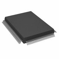
AD9888KSZ-140 Analog Devices Inc, AD9888KSZ-140 Datasheet - Page 29

AD9888KSZ-140
Manufacturer Part Number
AD9888KSZ-140
Description
IC FLAT PANEL INTERFACE 128-MQFP
Manufacturer
Analog Devices Inc
Datasheet
1.AD9888KSZ-205.pdf
(32 pages)
Specifications of AD9888KSZ-140
Applications
Graphic Cards, VGA Interfaces
Interface
2-Wire Serial
Voltage - Supply
3 V ~ 3.6 V
Package / Case
128-MQFP, 128-PQFP
Mounting Type
Surface Mount
Supply Current
200mA
Power Dissipation Pd
850mW
Supply Voltage Range
3V To 3.6V, 2.2V To 3.6V
Digital Ic Case Style
MQFP
No. Of Pins
128
Operating Temperature Range
0°C To +70°C
Svhc
No SVHC
Number Of Elements
3
Resolution
8Bit
Sample Rate
140MSPS
Input Polarity
Bipolar
Input Type
Voltage
Rated Input Volt
±0.25/±0.5V
Differential Input
No
Power Supply Requirement
Single
Single Supply Voltage (typ)
3.3V
Single Supply Voltage (min)
3V
Single Supply Voltage (max)
3.6V
Dual Supply Voltage (typ)
Not RequiredV
Dual Supply Voltage (min)
Not RequiredV
Dual Supply Voltage (max)
Not RequiredV
Power Dissipation
1.05W
Differential Linearity Error
±1.35LSB
Integral Nonlinearity Error
±2.5LSB
Operating Temp Range
0C to 70C
Operating Temperature Classification
Commercial
Mounting
Surface Mount
Pin Count
128
Package Type
MQFP
Input Signal Type
Single-Ended
Interface Type
2-wire, Serial
Rohs Compliant
Yes
Lead Free Status / RoHS Status
Lead free / RoHS Compliant
Lead Free Status / RoHS Status
Lead free / RoHS Compliant, Lead free / RoHS Compliant
Available stocks
Company
Part Number
Manufacturer
Quantity
Price
Company:
Part Number:
AD9888KSZ-140
Manufacturer:
AD
Quantity:
217
Company:
Part Number:
AD9888KSZ-140
Manufacturer:
ADI
Quantity:
482
Company:
Part Number:
AD9888KSZ-140
Manufacturer:
Analog Devices Inc
Quantity:
10 000
analog supply voltage. This can be mitigated by regulating the
analog supply, or at least PV
source (for example, from a 12 V supply).
It is also recommended to use a single ground plane for the
entire board. Experience has repeatedly shown that the noise
performance is the same or better with a single ground plane.
Using multiple ground planes can be detrimental because each
separate ground plane is smaller, and long ground loops can result.
In some cases, using separate ground planes is unavoidable. For
those cases, it is recommended to at least place a single ground
plane under the AD9888. The location of the split should be at
the receiver of the digital outputs. For this case, it is even more
important to place components wisely because the current loops
will be much longer (current takes the path of least resistance).
An example of a current loop: power plane => AD9888 =>
digital output trace => digital data receiver => digital ground
plane => analog ground plane.
PLL
Place the PLL loop filter components as close to the FILT pin
as possible.
Do not place any digital or other high frequency traces near
these components.
Use the values suggested in the data sheet with 10% tolerances
or less.
Outputs (Both Data and Clocks)
Try to minimize the trace length that the digital outputs have to
drive. Longer traces have higher capacitance, requiring more
current and causing more internal digital noise. Shorter traces
reduce the possibility of reflections.
REV. B
D
, from a different, cleaner, power
–29–
Adding a series resistor with a of value 22 Ω to 100 Ω can sup-
press reflections, reduce EMI, and reduce the current spikes
inside the AD9888. However, if 50 Ω traces are used on the
PCB, the data output should not need these resistors.
A 22 Ω resistor on the DATACK output should provide good
impedance matching that will reduce reflections. If EMI or
current spiking is a concern, we recommend using a lower drive
strength setting by adjusting Register 14H. If series resistors are
used, place them as close to the AD9888 pins as possible (but
avoid adding vias or extra length to the output trace in order to
get the resistors closer).
If possible, limit the capacitance that each of the digital outputs
drives to less than 10 pF. This can easily be accomplished by
keeping traces short and by connecting the outputs to only one
device. Loading the outputs with excessive capacitance will
increase the current transients inside of the AD9888 creating
more digital noise on its power supplies.
Digital Inputs
The digital inputs on the AD9888 were designed to work with
3.3 V signals, but are tolerant of 5.0 V signals. So, no extra
components need to be added if using 5.0 V logic.
Any noise that gets onto the Hsync input trace will add jitter to
the system. Therefore, minimize the trace length and do not run
any digital or other high frequency traces near it.
Voltage Reference
Bypass with a 0.1 µF capacitor. Place it as close to the AD9888
pin as possible. Make the ground connection as short as possible.
AD9888


