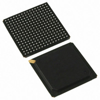
PI7C9X130DNDE Pericom Semiconductor, PI7C9X130DNDE Datasheet - Page 149

PI7C9X130DNDE
Manufacturer Part Number
PI7C9X130DNDE
Description
IC PCIE-PCIX BRIDGE 1PORT 256BGA
Manufacturer
Pericom Semiconductor
Specifications of PI7C9X130DNDE
Applications
PCI-to-PCI Bridge
Interface
SMBus (2-Wire/I²C)
Voltage - Supply
1.8V, 3.3V
Package / Case
256-PBGA
Mounting Type
Surface Mount
Operating Temperature (min)
-40C
Operating Temperature Classification
Industrial
Operating Temperature (max)
85C
Package Type
BGA
Rad Hardened
No
Lead Free Status / RoHS Status
Lead free / RoHS Compliant
Available stocks
Company
Part Number
Manufacturer
Quantity
Price
Company:
Part Number:
PI7C9X130DNDE
Manufacturer:
Pericom
Quantity:
135
Company:
Part Number:
PI7C9X130DNDE
Manufacturer:
NSC
Quantity:
70
14
PERICOM SEMICONDUCTOR - Confidential
14.1 INSTRUCTION REGISTER
IEEE 1149.1 COMPATIBLE JTAG CONTROLLER
14.2 BYPASS REGISTER
An IEEE 1149.1 compatible Test Access Port (TAP) controller and associated TAP pins are provided to
support boundary scan in PI7C9X130 for board-level continuity test and diagnostics. The TAP pins
assigned are TCK, TDI, TDO, TMS and TRST_L. All digital input, output, input/output pins are tested
except TAP pins.
The IEEE 1149.1 Test Logic consists of a TAP controller, an instruction register, and
a group of test data registers including Bypass and Boundary Scan registers. The TAP controller is a
synchronous 16-state machine driven by the Test Clock (TCK) and the
Test Mode Select (TMS) pins. An independent power on reset circuit is provided to ensure the machine
is in TEST_LOGIC_RESET state at power-up. The JTAG signal lines are not active when the PCI
resource is operating PCI bus cycles.
PI7C9X130 implements a 5-bit Instruction register to control the operation of the JTAG logic. The
defined instruction codes are shown in Table 14-1. Those bit combinations that are not listed are
equivalent to the BYPASS (11111) instruction:
Figure 14-16 Instruction Register Codes
The required bypass register (one-bit shift register) provides the shortest path between TDI and TDO
when a bypass instruction is in effect. This allows rapid movement of test data to and from other
components on the board. This path can be selected when no test operation is being performed on the
PI7C9X130.
This register identifies Pericom as the manufacturer of the device and details the part number and
revision number for the device.
Instruction
EXTEST
SAMPLE
HIGHZ
CLAMP
IDCODE
BYPASS
INT_SCAN
MEM_BIST
14.3 DEVICE ID REGISTER
Operation Code
(binary)
00000
00001
00101
00100
01100
11111
00010
01010
Page 149 of 165
Register
Selected
Boundary Scan
Boundary Scan
Bypass
Bypass
Device ID
Bypass
Internal Scan
Memory BIST
Operation
Samples inputs / pre-loads outputs
Tri-states output and I/O pins except TDO pin
Drives pins from boundary-scan register and
selects Bypass register for shifts
Accesses the Device ID register, to read
manufacturer ID, part number, and version
number
Memory BIST test
Drives / receives off-chip test data
Selected Bypass Register
Scan test
PCI EXPRESS TO PCI-X BRIDGE
Mar 2010 - Rev 2.0
PI7C9X130


