PI7C9X130DNDE Pericom Semiconductor, PI7C9X130DNDE Datasheet - Page 3
PI7C9X130DNDE
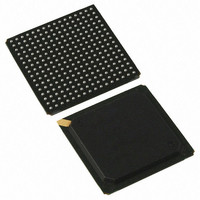
Manufacturer Part Number
PI7C9X130DNDE
Description
IC PCIE-PCIX BRIDGE 1PORT 256BGA
Manufacturer
Pericom Semiconductor
Specifications of PI7C9X130DNDE
Applications
PCI-to-PCI Bridge
Interface
SMBus (2-Wire/I²C)
Voltage - Supply
1.8V, 3.3V
Package / Case
256-PBGA
Mounting Type
Surface Mount
Operating Temperature (min)
-40C
Operating Temperature Classification
Industrial
Operating Temperature (max)
85C
Package Type
BGA
Rad Hardened
No
Lead Free Status / RoHS Status
Lead free / RoHS Compliant
Available stocks
Company
Part Number
Manufacturer
Quantity
Price
Company:

Part Number:
PI7C9X130DNDE
Manufacturer:
Pericom
Quantity:
135
Company:
Part Number:
PI7C9X130DNDE
Manufacturer:
NSC
Quantity:
70


REVISION HISTORY
PREFACE
PERICOM SEMICONDUCTOR - Confidential
Date
02/24/06
03/20/06
04/07/06
06/07/06
06/19/06
03/26/2007
04/18/2007
05/02/2007
05/15/2007
06/08/2007
07/13/2007
08/07/2007
09/28//2007
01/03/2008
04/21/2008
04/24/2008
08/08/2008
10/30/2008
7/1/2009
01/20/10
03/29/10
Revision Number
0.91
0.1
0.2
0.3
0.4
0.5
0.6
0.7
0.8
0.9
1.0
1.1
1.2
1.3
1.4
1.5
1.6
1.7
1.8
1.9
2.0
Update on configuration register bit definitions.
Add Absolute Maximum Ratings
Correct default setting for bit [31:30] of offset 68h
Completed non-transparent function for address 28h – 2Bh in the Configuration Register
Revised table 8-1 in section 8
Revised PCIe Base Specification Compliancy from 1.0a to 1.1
Corrected bit[13] offset 110h from reserved to “Advisory Non-Fatal Error Status”
Revised Ambient Temperature Maximum Ratings Compliancy
Revised Product Ordering Info
Added Asynchronous Clock Support to Section 19
Revised configuration register definitions:
Description
First Draft of PI7C9X130 Data Sheet
Correct INTA, B, C, D buffer type
Update configuration map and registers
Update JTAG chain order
Add PCI/PCI-X selection information
Correct typo of pin CLKRUN_L in pin assignment and JTAG section.
Correct pin description:
Map – section 7.1
Corrected pin HSEN (R3) in section 2.6 – Miscellaneous Signals. Should read tie LOW
if Hot Swap is not used instead of tie HIGH
Corrected pin HSSW (T3) in section 2.6 – Miscellaneous Signals.
“Tied high if hot swap function is not used.”
Changed Logos and some font types
Corrected Pin #’s of GNT_L[1], GNT_L[2], GNT_[3], GNT_[4], GNT_[5] on
Table 14-1JTAG Boundary Scan Register Definition
Recommendation of Pull-up Resistor for PI7C9X130 Control Signals added to section
16.3 of PI7C9X130 Datasheets; pin numbers of SMBCLK and SMBDAT are corrected
under section 5.2.
Updated to revision D
Added package thermal data. RREF pin description change.
Removed CDM information
Added Power-Up Sequencing Description
Added Extended Configuration Access / Data Register under section 7.1 and 7.4
Revised Section 9 Clock Scheme
1)
2)
3)
4)
5)
1)
2)
3)
4)
5)
6)
Address bit[5] corrected to equal 0
Address bit[4] corrected to equal GPIO[3]
Page 3 of 165
1.
2.
Bit [10, 7:2] of offset 40h
Bit [31:30] of offset 68h
Bit [0] of offset 70h
Bit [23:22] of offset 94h
Bit [7:1] of offset 164h
7.4.31 bit[5:4] and bit[7:6] of PCI Data Buffering Control Register )Offset
40h)
7.4.87 Extended Configuration Access Address Register (Offset E0h)
7.4.88 Extended Configuration Access Data Register (Offset E4h)
7.4.129 bit[30] of Replay and Acknowledge Latency Timers (Offset 310h)
7.5.24 bit[5:4] and bit[7:6] of PCI Data Buffering Control Register )Offset
40h)
7.5.135 bit[30] of Replay and Acknowledge Latency Timers (Offset 310h)
REQ_L as GPI and GNT_L as GPO
CLKOUT [8:0] as CLKOUT [6:0]
Added PCIX Clock Detection to Chapter 9, Clock Scheme.
PCI EXPRESS TO PCI-X BRIDGE
Mar 2010 - Rev 2.0
Remove
PI7C9X130
Related parts for PI7C9X130DNDE
Image
Part Number
Description
Manufacturer
Datasheet
Request
R

Part Number:
Description:
Fast CMOS bus interface register
Manufacturer:
Pericom Semiconductor
Datasheet:
Part Number:
Description:
4-bit,4-port bus exchange switch
Manufacturer:
Pericom Semiconductor
Datasheet:
Part Number:
Description:
Manufacturer:
Pericom Semiconductor
Datasheet:
Part Number:
Description:
Manufacturer:
Pericom Semiconductor
Datasheet:
Part Number:
Description:
Manufacturer:
Pericom Semiconductor
Datasheet:
Part Number:
Description:
Manufacturer:
Pericom Semiconductor
Datasheet:
Part Number:
Description:
Manufacturer:
Pericom Semiconductor
Datasheet:
Part Number:
Description:
Manufacturer:
Pericom Semiconductor
Datasheet:
Part Number:
Description:
Manufacturer:
Pericom Semiconductor
Datasheet:
Part Number:
Description:
Manufacturer:
Pericom Semiconductor
Datasheet:
Part Number:
Description:
Manufacturer:
Pericom Semiconductor
Datasheet:
Part Number:
Description:
Manufacturer:
Pericom Semiconductor
Datasheet:
Part Number:
Description:
Manufacturer:
Pericom Semiconductor
Datasheet:
Part Number:
Description:
Manufacturer:
Pericom Semiconductor
Datasheet: