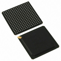
PI7C9X130DNDE Pericom Semiconductor, PI7C9X130DNDE Datasheet - Page 150

PI7C9X130DNDE
Manufacturer Part Number
PI7C9X130DNDE
Description
IC PCIE-PCIX BRIDGE 1PORT 256BGA
Manufacturer
Pericom Semiconductor
Specifications of PI7C9X130DNDE
Applications
PCI-to-PCI Bridge
Interface
SMBus (2-Wire/I²C)
Voltage - Supply
1.8V, 3.3V
Package / Case
256-PBGA
Mounting Type
Surface Mount
Operating Temperature (min)
-40C
Operating Temperature Classification
Industrial
Operating Temperature (max)
85C
Package Type
BGA
Rad Hardened
No
Lead Free Status / RoHS Status
Lead free / RoHS Compliant
Available stocks
Company
Part Number
Manufacturer
Quantity
Price
Company:
Part Number:
PI7C9X130DNDE
Manufacturer:
Pericom
Quantity:
135
Company:
Part Number:
PI7C9X130DNDE
Manufacturer:
NSC
Quantity:
70
- Current page: 150 of 165
- Download datasheet (2Mb)
14.4 BOUNDARY SCAN REGISTER
14.5 JTAG BOUNDARY SCAN REGISTER ORDER
PERICOM SEMICONDUCTOR - Confidential
Figure 14-17 JTAG Device ID Register
The boundary scan register has a set of serial shift-register cells. A chain of boundary scan cells is
formed by connected the internal signal of the PI7C9X130 package pins. The VDD, VSS, and JTAG
pins are not in the boundary scan chain. The input to the shift register is TDI and the output from the shift
register is TDO. There are 4 different types of boundary scan cells, based on the function of each signal
pin.
The boundary scan register cells are dedicated logic and do not have any system function. Data may be
loaded into the boundary scan register master cells from the device input pins and output pin-drivers in
parallel by the mandatory SAMPLE and EXTEST instructions. Parallel loading takes place on the rising
edge of TCK.
Table 14-1 JTAG Boundary Scan Register Definition
Bit
31:28
27:12
11:1
0
Boundary
Register
Number
Scan
10
11
12
13
14
15
16
17
18
0
1
2
3
4
5
6
7
8
9
-
Type
RO
RO
RO
RO
Pin Name
GPIO [6]
CBE [0]
AD [0]
AD [1]
AD [2]
AD [3]
AD [4]
AD [5]
AD [6]
AD [7]
-
-
-
-
-
-
-
-
Value
00h
E130h
23Fh
1b
Page 150 of 165
Ball Location
K13
K14
K15
K16
L15
L16
J13
J14
J15
J16
-
-
-
-
-
-
-
-
-
Description
Last 4 digits (hex) of the die part number
Pericom identifier assigned by JEDEC
Fixed bit equal to 1’b1
Version number
CONTROL
CONTROL
CONTROL
CONTROL
CONTROL
CONTROL
CONTROL
CONTROL
CONTROL
BIDIR
BIDIR
BIDIR
BIDIR
BIDIR
BIDIR
BIDIR
BIDIR
BIDIR
BIDIR
Type
PCI EXPRESS TO PCI-X BRIDGE
Tri-state Control Cell
Mar 2010 - Rev 2.0
11
13
15
17
19
1
3
5
7
9
-
-
-
-
-
-
-
-
-
PI7C9X130
Related parts for PI7C9X130DNDE
Image
Part Number
Description
Manufacturer
Datasheet
Request
R
Part Number:
Description:
Fast CMOS bus interface register
Manufacturer:
Pericom Semiconductor
Datasheet:
Part Number:
Description:
4-bit,4-port bus exchange switch
Manufacturer:
Pericom Semiconductor
Datasheet:
Part Number:
Description:
Manufacturer:
Pericom Semiconductor
Datasheet:
Part Number:
Description:
Manufacturer:
Pericom Semiconductor
Datasheet:
Part Number:
Description:
Manufacturer:
Pericom Semiconductor
Datasheet:
Part Number:
Description:
Manufacturer:
Pericom Semiconductor
Datasheet:
Part Number:
Description:
Manufacturer:
Pericom Semiconductor
Datasheet:
Part Number:
Description:
Manufacturer:
Pericom Semiconductor
Datasheet:
Part Number:
Description:
Manufacturer:
Pericom Semiconductor
Datasheet:
Part Number:
Description:
Manufacturer:
Pericom Semiconductor
Datasheet:
Part Number:
Description:
Manufacturer:
Pericom Semiconductor
Datasheet:
Part Number:
Description:
Manufacturer:
Pericom Semiconductor
Datasheet:
Part Number:
Description:
Manufacturer:
Pericom Semiconductor
Datasheet:
Part Number:
Description:
Manufacturer:
Pericom Semiconductor
Datasheet:


