TMPSNS-RTD1 Microchip Technology, TMPSNS-RTD1 Datasheet - Page 170
TMPSNS-RTD1
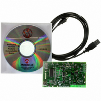
Manufacturer Part Number
TMPSNS-RTD1
Description
BOARD EVAL PT100 RTD TEMP SENSOR
Manufacturer
Microchip Technology
Datasheets
1.MCP3301-CIMS.pdf
(32 pages)
2.PCM18XR1.pdf
(438 pages)
3.MCP6S22DM-PICTL.pdf
(43 pages)
4.TMPSNS-RTD1.pdf
(26 pages)
Specifications of TMPSNS-RTD1
Sensor Type
Temperature
Interface
USB
Embedded
Yes, MCU, 8-Bit
Utilized Ic / Part
MCP3301, MCP6S26, PIC18F2550
Processor To Be Evaluated
MCP6S26, MCP3301, MCP6024, MCP41010, PIC18F2550, TC1071, MCP6002
Data Bus Width
12 bit
Interface Type
USB
Lead Free Status / RoHS Status
Not applicable / Not applicable
Voltage - Supply
-
Sensitivity
-
Sensing Range
-
Lead Free Status / RoHS Status
Lead free / RoHS Compliant, Not applicable / Not applicable


PIC18F2455/2550/4455/4550
REGISTER 17-2:
There are 6 signals from the module to communicate
with and control an external transceiver:
• VM: Input from the single-ended D- line
• VP: Input from the single-ended D+ line
• RCV: Input from the differential receiver
• VMO: Output to the differential line driver
• VPO: Output to the differential line driver
• UOE: Output enable
DS39632E-page 168
bit 7
Legend:
R = Readable bit
-n = Value at POR
bit 7
bit 6
bit 5
bit 4
bit 3
bit 2
bit 1-0
Note 1:
UTEYE
R/W-0
2:
3:
If UTRDIS is set, the UOE signal will be active independent of the UOEMON bit setting.
The UPUEN, UTRDIS and FSEN bits should never be changed while the USB module is enabled. These
values must be preconfigured prior to enabling the module.
This bit is only valid when the on-chip transceiver is active (UTRDIS = 0); otherwise, it is ignored.
UTEYE: USB Eye Pattern Test Enable bit
1 = Eye pattern test enabled
0 = Eye pattern test disabled
UOEMON: USB OE Monitor Enable bit
1 = UOE signal active; it indicates intervals during which the D+/D- lines are driving
0 = UOE signal inactive
Unimplemented: Read as ‘0’
UPUEN: USB On-Chip Pull-up Enable bit
1 = On-chip pull-up enabled (pull-up on D+ with FSEN = 1 or D- with FSEN = 0)
0 = On-chip pull-up disabled
UTRDIS: On-Chip Transceiver Disable bit
1 = On-chip transceiver disabled; digital transceiver interface enabled
0 = On-chip transceiver active
FSEN: Full-Speed Enable bit
1 = Full-speed device: controls transceiver edge rates; requires input clock at 48 MHz
0 = Low-speed device: controls transceiver edge rates; requires input clock at 6 MHz
PPB1:PPB0: Ping-Pong Buffers Configuration bits
11 = Even/Odd ping-pong buffers enabled for Endpoints 1 to 15
10 = Even/Odd ping-pong buffers enabled for all endpoints
01 = Even/Odd ping-pong buffer enabled for OUT Endpoint 0
00 = Even/Odd ping-pong buffers disabled
UOEMON
R/W-0
UCFG: USB CONFIGURATION REGISTER
(1)
W = Writable bit
‘1’ = Bit is set
U-0
—
(2)
UPUEN
R/W-0
(2,3)
(1)
(2,3)
(2)
U = Unimplemented bit, read as ‘0’
‘0’ = Bit is cleared
UTRDIS
R/W-0
The VPO and VMO signals are outputs from the SIE to
the external transceiver. The RCV signal is the output
from the external transceiver to the SIE; it represents
the differential signals from the serial bus translated
into a single pulse train. The VM and VP signals are
used to report conditions on the serial bus to the SIE
that can’t be captured with the RCV signal. The
combinations of states of these signals and their
interpretation are listed in Table 17-1 and Table 17-2.
(2)
FSEN
R/W-0
(2)
© 2009 Microchip Technology Inc.
x = Bit is unknown
R/W-0
PPB1
R/W-0
PPB0
bit 0
Related parts for TMPSNS-RTD1
Image
Part Number
Description
Manufacturer
Datasheet
Request
R

Part Number:
Description:
Manufacturer:
Microchip Technology Inc.
Datasheet:
Part Number:
Description:
Manufacturer:
Microchip Technology Inc.
Datasheet:
Part Number:
Description:
Manufacturer:
Microchip Technology Inc.
Datasheet:
Part Number:
Description:
Manufacturer:
Microchip Technology Inc.
Datasheet:
Part Number:
Description:
Manufacturer:
Microchip Technology Inc.
Datasheet:
Part Number:
Description:
Manufacturer:
Microchip Technology Inc.
Datasheet:
Part Number:
Description:
Manufacturer:
Microchip Technology Inc.
Datasheet:
Part Number:
Description:
Manufacturer:
Microchip Technology Inc.
Datasheet: