TMPSNS-RTD1 Microchip Technology, TMPSNS-RTD1 Datasheet - Page 71
TMPSNS-RTD1
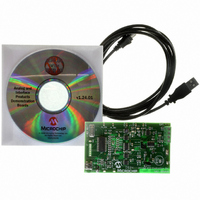
Manufacturer Part Number
TMPSNS-RTD1
Description
BOARD EVAL PT100 RTD TEMP SENSOR
Manufacturer
Microchip Technology
Datasheets
1.MCP3301-CIMS.pdf
(32 pages)
2.PCM18XR1.pdf
(438 pages)
3.MCP6S22DM-PICTL.pdf
(43 pages)
4.TMPSNS-RTD1.pdf
(26 pages)
Specifications of TMPSNS-RTD1
Sensor Type
Temperature
Interface
USB
Embedded
Yes, MCU, 8-Bit
Utilized Ic / Part
MCP3301, MCP6S26, PIC18F2550
Processor To Be Evaluated
MCP6S26, MCP3301, MCP6024, MCP41010, PIC18F2550, TC1071, MCP6002
Data Bus Width
12 bit
Interface Type
USB
Lead Free Status / RoHS Status
Not applicable / Not applicable
Voltage - Supply
-
Sensitivity
-
Sensing Range
-
Lead Free Status / RoHS Status
Lead free / RoHS Compliant, Not applicable / Not applicable


TABLE 5-2:
© 2009 Microchip Technology Inc.
TOSU
TOSH
TOSL
STKPTR
PCLATU
PCLATH
PCL
TBLPTRU
TBLPTRH
TBLPTRL
TABLAT
PRODH
PRODL
INTCON
INTCON2
INTCON3
INDF0
POSTINC0
POSTDEC0
PREINC0
PLUSW0
FSR0H
FSR0L
WREG
INDF1
POSTINC1
POSTDEC1
PREINC1
PLUSW1
FSR1H
FSR1L
BSR
INDF2
POSTINC2
POSTDEC2
PREINC2
PLUSW2
FSR2H
FSR2L
STATUS
TMR0H
TMR0L
T0CON
Legend:
Note
File Name
1:
2:
3:
4:
5:
6:
7:
x = unknown, u = unchanged, - = unimplemented, q = value depends on condition. Shaded cells are unimplemented, read as ‘0’.
Bit 21 of the TBLPTRU allows access to the device Configuration bits.
The SBOREN bit is only available when BOREN<1:0> = 01; otherwise, the bit reads as ‘0’.
These registers and/or bits are not implemented on 28-pin devices and are read as ‘0’. Reset values are shown for 40/44-pin devices;
individual unimplemented bits should be interpreted as ‘-’.
RA6 is configured as a port pin based on various primary oscillator modes. When the port pin is disabled, all of the associated bits read ‘0’.
RE3 is only available as a port pin when the MCLRE Configuration bit is clear; otherwise, the bit reads as ‘0’.
RC5 and RC4 are only available as port pins when the USB module is disabled (UCON<3> = 0).
I
2
Top-of-Stack High Byte (TOS<15:8>)
Top-of-Stack Low Byte (TOS<7:0>)
Holding Register for PC<15:8>
PC Low Byte (PC<7:0>)
Program Memory Table Pointer High Byte (TBLPTR<15:8>)
Program Memory Table Pointer Low Byte (TBLPTR<7:0>)
Program Memory Table Latch
Product Register High Byte
Product Register Low Byte
Uses contents of FSR0 to address data memory – value of FSR0 not changed (not a physical register)
Uses contents of FSR0 to address data memory – value of FSR0 post-incremented (not a physical register)
Uses contents of FSR0 to address data memory – value of FSR0 post-decremented (not a physical register)
Uses contents of FSR0 to address data memory – value of FSR0 pre-incremented (not a physical register)
Uses contents of FSR0 to address data memory – value of FSR0 pre-incremented (not a physical register) –
value of FSR0 offset by W
Indirect Data Memory Address Pointer 0 Low Byte
Working Register
Uses contents of FSR1 to address data memory – value of FSR1 not changed (not a physical register)
Uses contents of FSR1 to address data memory – value of FSR1 post-incremented (not a physical register)
Uses contents of FSR1 to address data memory – value of FSR1 post-decremented (not a physical register)
Uses contents of FSR1 to address data memory – value of FSR1 pre-incremented (not a physical register)
Uses contents of FSR1 to address data memory – value of FSR1 pre-incremented (not a physical register) –
value of FSR1 offset by W
Indirect Data Memory Address Pointer 1 Low Byte
Uses contents of FSR2 to address data memory – value of FSR2 not changed (not a physical register)
Uses contents of FSR2 to address data memory – value of FSR2 post-incremented (not a physical register)
Uses contents of FSR2 to address data memory – value of FSR2 post-decremented (not a physical register)
Uses contents of FSR2 to address data memory – value of FSR2 pre-incremented (not a physical register)
Uses contents of FSR2 to address data memory – value of FSR2 pre-incremented (not a physical register) –
value of FSR2 offset by W
Indirect Data Memory Address Pointer 2 Low Byte
Timer0 Register High Byte
Timer0 Register Low Byte
C™ Slave mode only.
GIE/GIEH
TMR0ON
STKFUL
INT2IP
RBPU
Bit 7
—
—
—
—
—
—
—
—
REGISTER FILE SUMMARY
PEIE/GIEL
INTEDG0
STKUNF
T08BIT
INT1IP
Bit 6
—
—
—
—
—
—
—
—
INTEDG1
TMR0IE
bit 21
T0CS
Bit 5
—
—
—
—
—
—
—
—
—
(1)
PIC18F2455/2550/4455/4550
Top-of-Stack Upper Byte (TOS<20:16>)
Holding Register for PC<20:16>
Program Memory Table Pointer Upper Byte (TBLPTR<20:16>)
INTEDG2
INT0IE
INT2IE
T0SE
Bit 4
SP4
—
—
—
—
N
Indirect Data Memory Address Pointer 0 High Byte
Indirect Data Memory Address Pointer 1 High Byte
Bank Select Register
Indirect Data Memory Address Pointer 2 High Byte
INT1IE
RBIE
Bit 3
PSA
SP3
OV
—
TMR0IF
TMR0IP
T0PS2
Bit 2
SP2
—
Z
INT0IF
INT2IF
T0PS1
Bit 1
SP1
DC
—
INT1IF
T0PS0
RBIP
Bit 0
RBIF
SP0
C
DS39632E-page 69
---0 0000
0000 0000
0000 0000
00-0 0000
---0 0000
0000 0000
0000 0000
--00 0000
0000 0000
0000 0000
0000 0000
xxxx xxxx
xxxx xxxx
0000 000x
1111 -1-1
11-0 0-00
---- 0000
xxxx xxxx
xxxx xxxx
---- 0000
xxxx xxxx
---- 0000
---- 0000
xxxx xxxx
---x xxxx
0000 0000
xxxx xxxx
1111 1111
POR, BOR
Value on
N/A
N/A
N/A
N/A
N/A
N/A
N/A
N/A
N/A
N/A
N/A
N/A
N/A
N/A
N/A
on page
Details
53, 101
53, 102
53, 103
54, 129
54, 129
54, 127
53, 60
53, 60
53, 60
53, 61
53, 60
53, 60
53, 60
53, 84
53, 84
53, 84
53, 84
53, 97
53, 97
53, 75
53, 76
53, 76
53, 76
53, 76
53, 75
53, 75
53, 75
53, 76
53, 76
53, 76
53, 76
53, 75
53, 75
54, 65
54, 75
54, 76
54, 76
54, 76
54, 76
54, 75
54, 75
54, 73
53
Related parts for TMPSNS-RTD1
Image
Part Number
Description
Manufacturer
Datasheet
Request
R

Part Number:
Description:
Manufacturer:
Microchip Technology Inc.
Datasheet:
Part Number:
Description:
Manufacturer:
Microchip Technology Inc.
Datasheet:
Part Number:
Description:
Manufacturer:
Microchip Technology Inc.
Datasheet:
Part Number:
Description:
Manufacturer:
Microchip Technology Inc.
Datasheet:
Part Number:
Description:
Manufacturer:
Microchip Technology Inc.
Datasheet:
Part Number:
Description:
Manufacturer:
Microchip Technology Inc.
Datasheet:
Part Number:
Description:
Manufacturer:
Microchip Technology Inc.
Datasheet:
Part Number:
Description:
Manufacturer:
Microchip Technology Inc.
Datasheet: