TMPSNS-RTD1 Microchip Technology, TMPSNS-RTD1 Datasheet - Page 267
TMPSNS-RTD1
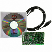
Manufacturer Part Number
TMPSNS-RTD1
Description
BOARD EVAL PT100 RTD TEMP SENSOR
Manufacturer
Microchip Technology
Datasheets
1.MCP3301-CIMS.pdf
(32 pages)
2.PCM18XR1.pdf
(438 pages)
3.MCP6S22DM-PICTL.pdf
(43 pages)
4.TMPSNS-RTD1.pdf
(26 pages)
Specifications of TMPSNS-RTD1
Sensor Type
Temperature
Interface
USB
Embedded
Yes, MCU, 8-Bit
Utilized Ic / Part
MCP3301, MCP6S26, PIC18F2550
Processor To Be Evaluated
MCP6S26, MCP3301, MCP6024, MCP41010, PIC18F2550, TC1071, MCP6002
Data Bus Width
12 bit
Interface Type
USB
Lead Free Status / RoHS Status
Not applicable / Not applicable
Voltage - Supply
-
Sensitivity
-
Sensing Range
-
Lead Free Status / RoHS Status
Lead free / RoHS Compliant, Not applicable / Not applicable


21.0
The Analog-to-Digital (A/D) converter module has
10 inputs for the 28-pin devices and 13 for the
40/44-pin devices. This module allows conversion of an
analog input signal to a corresponding 10-bit digital
number.
The module has five registers:
• A/D Result High Register (ADRESH)
• A/D Result Low Register (ADRESL)
• A/D Control Register 0 (ADCON0)
• A/D Control Register 1 (ADCON1)
• A/D Control Register 2 (ADCON2)
REGISTER 21-1:
© 2009 Microchip Technology Inc.
bit 7
Legend:
R = Readable bit
-n = Value at POR
bit 7-6
bit 5-2
bit 1
bit 0
Note 1:
U-0
—
2:
10-BIT ANALOG-TO-DIGITAL
CONVERTER (A/D) MODULE
These channels are not implemented on 28-pin devices.
Performing a conversion on unimplemented channels will return a floating input measurement.
Unimplemented: Read as ‘0’
CHS3:CHS0: Analog Channel Select bits
0000 = Channel 0 (AN0)
0001 = Channel 1 (AN1)
0010 = Channel 2 (AN2)
0011 = Channel 3 (AN3)
0100 = Channel 4 (AN4)
0101 = Channel 5 (AN5)
0110 = Channel 6 (AN6)
0111 = Channel 7 (AN7)
1000 = Channel 8 (AN8)
1001 = Channel 9 (AN9)
1010 = Channel 10 (AN10)
1011 = Channel 11 (AN11)
1100 = Channel 12 (AN12)
1101 = Unimplemented
1110 = Unimplemented
1111 = Unimplemented
GO/DONE: A/D Conversion Status bit
When ADON = 1:
1 = A/D conversion in progress
0 = A/D Idle
ADON: A/D On bit
1 = A/D converter module is enabled
0 = A/D converter module is disabled
U-0
—
ADCON0: A/D CONTROL REGISTER 0
W = Writable bit
‘1’ = Bit is set
R/W-0
CHS3
(2)
(2)
(2)
(1,2)
(1,2)
(1,2)
PIC18F2455/2550/4455/4550
R/W-0
CHS2
U = Unimplemented bit, read as ‘0’
‘0’ = Bit is cleared
R/W-0
CHS1
The ADCON0 register, shown in Register 21-1,
controls the operation of the A/D module. The
ADCON1 register, shown in Register 21-2, configures
the functions of the port pins. The ADCON2 register,
shown in Register 21-3, configures the A/D clock
source, programmed acquisition time and justification.
R/W-0
CHS0
x = Bit is unknown
GO/DONE
R/W-0
DS39632E-page 265
R/W-0
ADON
bit 0
Related parts for TMPSNS-RTD1
Image
Part Number
Description
Manufacturer
Datasheet
Request
R

Part Number:
Description:
Manufacturer:
Microchip Technology Inc.
Datasheet:
Part Number:
Description:
Manufacturer:
Microchip Technology Inc.
Datasheet:
Part Number:
Description:
Manufacturer:
Microchip Technology Inc.
Datasheet:
Part Number:
Description:
Manufacturer:
Microchip Technology Inc.
Datasheet:
Part Number:
Description:
Manufacturer:
Microchip Technology Inc.
Datasheet:
Part Number:
Description:
Manufacturer:
Microchip Technology Inc.
Datasheet:
Part Number:
Description:
Manufacturer:
Microchip Technology Inc.
Datasheet:
Part Number:
Description:
Manufacturer:
Microchip Technology Inc.
Datasheet: