TMPSNS-RTD1 Microchip Technology, TMPSNS-RTD1 Datasheet - Page 94
TMPSNS-RTD1
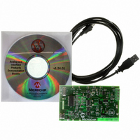
Manufacturer Part Number
TMPSNS-RTD1
Description
BOARD EVAL PT100 RTD TEMP SENSOR
Manufacturer
Microchip Technology
Datasheets
1.MCP3301-CIMS.pdf
(32 pages)
2.PCM18XR1.pdf
(438 pages)
3.MCP6S22DM-PICTL.pdf
(43 pages)
4.TMPSNS-RTD1.pdf
(26 pages)
Specifications of TMPSNS-RTD1
Sensor Type
Temperature
Interface
USB
Embedded
Yes, MCU, 8-Bit
Utilized Ic / Part
MCP3301, MCP6S26, PIC18F2550
Processor To Be Evaluated
MCP6S26, MCP3301, MCP6024, MCP41010, PIC18F2550, TC1071, MCP6002
Data Bus Width
12 bit
Interface Type
USB
Lead Free Status / RoHS Status
Not applicable / Not applicable
Voltage - Supply
-
Sensitivity
-
Sensing Range
-
Lead Free Status / RoHS Status
Lead free / RoHS Compliant, Not applicable / Not applicable


PIC18F2455/2550/4455/4550
REGISTER 7-1:
DS39632E-page 92
bit 7
Legend:
R = Readable bit
-n = Value at POR
bit 7
bit 6
bit 5
bit 4
bit 3
bit 2
bit 1
bit 0
Note 1:
EEPGD
R/W-x
When a WRERR occurs, the EEPGD and CFGS bits are not cleared. This allows tracing of the error
condition.
EEPGD: Flash Program or Data EEPROM Memory Select bit
1 = Access Flash program memory
0 = Access data EEPROM memory
CFGS: Flash Program/Data EEPROM or Configuration Select bit
1 = Access Configuration registers
0 = Access Flash program or data EEPROM memory
Unimplemented: Read as ‘0’
FREE: Flash Row Erase Enable bit
1 = Erase the program memory row addressed by TBLPTR on the next WR command (cleared by
0 = Perform write-only
WRERR: Flash Program/Data EEPROM Error Flag bit
1 = A write operation is prematurely terminated (any Reset during self-timed programming in normal
0 = The write operation completed
WREN: Flash Program/Data EEPROM Write Enable bit
1 = Allows write cycles to Flash program/data EEPROM
0 = Inhibits write cycles to Flash program/data EEPROM
WR: Write Control bit
1 = Initiates a data EEPROM erase/write cycle or a program memory erase cycle or write cycle
0 = Write cycle to the EEPROM is complete
RD: Read Control bit
1 = Initiates an EEPROM read (Read takes one cycle. RD is cleared in hardware. The RD bit can only
0 = Does not initiate an EEPROM read
R/W-x
CFGS
completion of erase operation)
operation or an improper write attempt)
(The operation is self-timed and the bit is cleared by hardware once write is complete.
The WR bit can only be set (not cleared) in software.)
be set (not cleared) in software. RD bit cannot be set when EEPGD = 1 or CFGS = 1.)
EECON1: DATA EEPROM CONTROL REGISTER 1
S = Settable bit
W = Writable bit
‘1’ = Bit is set
U-0
—
R/W-0
FREE
U = Unimplemented bit, read as ‘0’
‘0’ = Bit is cleared
WRERR
R/W-x
(1)
(1)
WREN
R/W-0
© 2009 Microchip Technology Inc.
x = Bit is unknown
R/S-0
WR
R/S-0
RD
bit 0
Related parts for TMPSNS-RTD1
Image
Part Number
Description
Manufacturer
Datasheet
Request
R

Part Number:
Description:
Manufacturer:
Microchip Technology Inc.
Datasheet:
Part Number:
Description:
Manufacturer:
Microchip Technology Inc.
Datasheet:
Part Number:
Description:
Manufacturer:
Microchip Technology Inc.
Datasheet:
Part Number:
Description:
Manufacturer:
Microchip Technology Inc.
Datasheet:
Part Number:
Description:
Manufacturer:
Microchip Technology Inc.
Datasheet:
Part Number:
Description:
Manufacturer:
Microchip Technology Inc.
Datasheet:
Part Number:
Description:
Manufacturer:
Microchip Technology Inc.
Datasheet:
Part Number:
Description:
Manufacturer:
Microchip Technology Inc.
Datasheet: