TMPSNS-RTD1 Microchip Technology, TMPSNS-RTD1 Datasheet - Page 229
TMPSNS-RTD1
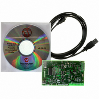
Manufacturer Part Number
TMPSNS-RTD1
Description
BOARD EVAL PT100 RTD TEMP SENSOR
Manufacturer
Microchip Technology
Datasheets
1.MCP3301-CIMS.pdf
(32 pages)
2.PCM18XR1.pdf
(438 pages)
3.MCP6S22DM-PICTL.pdf
(43 pages)
4.TMPSNS-RTD1.pdf
(26 pages)
Specifications of TMPSNS-RTD1
Sensor Type
Temperature
Interface
USB
Embedded
Yes, MCU, 8-Bit
Utilized Ic / Part
MCP3301, MCP6S26, PIC18F2550
Processor To Be Evaluated
MCP6S26, MCP3301, MCP6024, MCP41010, PIC18F2550, TC1071, MCP6002
Data Bus Width
12 bit
Interface Type
USB
Lead Free Status / RoHS Status
Not applicable / Not applicable
Voltage - Supply
-
Sensitivity
-
Sensing Range
-
Lead Free Status / RoHS Status
Lead free / RoHS Compliant, Not applicable / Not applicable


19.4.6.1
The master device generates all of the serial clock
pulses and the Start and Stop conditions. A transfer is
ended with a Stop condition or with a Repeated Start
condition. Since the Repeated Start condition is also
the beginning of the next serial transfer, the I
not be released.
In Master Transmitter mode, serial data is output
through SDA, while SCL outputs the serial clock. The
first byte transmitted contains the slave address of the
receiving device (seven bits) and the Read/Write (R/W)
bit. In this case, the R/W bit will be logic ‘0’. Serial data
is transmitted eight bits at a time. After each byte is
transmitted, an Acknowledge bit is received. Start and
Stop conditions are output to indicate the beginning
and the end of a serial transfer.
In Master Receive mode, the first byte transmitted con-
tains the slave address of the transmitting device
(7 bits) and the R/W bit. In this case, the R/W bit will be
logic ‘1’ Thus, the first byte transmitted is a 7-bit slave
address followed by a ‘1’ to indicate the receive bit.
Serial data is received via SDA, while SCL outputs the
serial clock. Serial data is received eight bits at a time.
After each byte is received, an Acknowledge bit is
transmitted. Start and Stop conditions indicate the
beginning and end of transmission.
The Baud Rate Generator used for the SPI mode
operation is used to set the SCL clock frequency for
either 100 kHz, 400 kHz or 1 MHz I
Section 19.4.7 “Baud Rate” for more detail.
© 2009 Microchip Technology Inc.
I
2
C Master Mode Operation
2
C operation. See
2
C bus will
PIC18F2455/2550/4455/4550
A typical transmit sequence would go as follows:
1.
2.
3.
4.
5.
6.
7.
8.
9.
10. The MSSP module generates an interrupt at the
11. The user generates a Stop condition by setting
12. Interrupt is generated once the Stop condition is
The user generates a Start condition by setting
the Start Enable bit, SEN (SSPCON2<0>).
SSPIF is set. The MSSP module will wait the
required start time before any other operation
takes place.
The user loads the SSPBUF with the slave
address to transmit.
Address is shifted out the SDA pin until all eight
bits are transmitted.
The MSSP module shifts in the ACK bit from the
slave device and writes its value into the
SSPCON2 register (SSPCON2<6>).
The MSSP module generates an interrupt at the
end of the ninth clock cycle by setting the SSPIF
bit.
The user loads the SSPBUF with eight bits of
data.
Data is shifted out the SDA pin until all eight bits
are transmitted.
The MSSP module shifts in the ACK bit from the
slave device and writes its value into the
SSPCON2 register (SSPCON2<6>).
end of the ninth clock cycle by setting the SSPIF
bit.
the Stop Enable bit, PEN (SSPCON2<2>).
complete.
DS39632E-page 227
Related parts for TMPSNS-RTD1
Image
Part Number
Description
Manufacturer
Datasheet
Request
R

Part Number:
Description:
Manufacturer:
Microchip Technology Inc.
Datasheet:
Part Number:
Description:
Manufacturer:
Microchip Technology Inc.
Datasheet:
Part Number:
Description:
Manufacturer:
Microchip Technology Inc.
Datasheet:
Part Number:
Description:
Manufacturer:
Microchip Technology Inc.
Datasheet:
Part Number:
Description:
Manufacturer:
Microchip Technology Inc.
Datasheet:
Part Number:
Description:
Manufacturer:
Microchip Technology Inc.
Datasheet:
Part Number:
Description:
Manufacturer:
Microchip Technology Inc.
Datasheet:
Part Number:
Description:
Manufacturer:
Microchip Technology Inc.
Datasheet: