TMPSNS-RTD1 Microchip Technology, TMPSNS-RTD1 Datasheet - Page 40
TMPSNS-RTD1
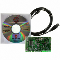
Manufacturer Part Number
TMPSNS-RTD1
Description
BOARD EVAL PT100 RTD TEMP SENSOR
Manufacturer
Microchip Technology
Datasheets
1.MCP3301-CIMS.pdf
(32 pages)
2.PCM18XR1.pdf
(438 pages)
3.MCP6S22DM-PICTL.pdf
(43 pages)
4.TMPSNS-RTD1.pdf
(26 pages)
Specifications of TMPSNS-RTD1
Sensor Type
Temperature
Interface
USB
Embedded
Yes, MCU, 8-Bit
Utilized Ic / Part
MCP3301, MCP6S26, PIC18F2550
Processor To Be Evaluated
MCP6S26, MCP3301, MCP6024, MCP41010, PIC18F2550, TC1071, MCP6002
Data Bus Width
12 bit
Interface Type
USB
Lead Free Status / RoHS Status
Not applicable / Not applicable
Voltage - Supply
-
Sensitivity
-
Sensing Range
-
Lead Free Status / RoHS Status
Lead free / RoHS Compliant, Not applicable / Not applicable


PIC18F2455/2550/4455/4550
3.2.3
In RC_RUN mode, the CPU and peripherals are
clocked from the internal oscillator block using the
INTOSC multiplexer; the primary clock is shut down.
When using the INTRC source, this mode provides the
best power conservation of all the Run modes while still
executing code. It works well for user applications
which are not highly timing sensitive or do not require
high-speed clocks at all times.
If the primary clock source is the internal oscillator
block (either INTRC or INTOSC), there are no distin-
guishable differences between the PRI_RUN and
RC_RUN modes during execution. However, a clock
switch delay will occur during entry to and exit from
RC_RUN mode. Therefore, if the primary clock source
is the internal oscillator block, the use of RC_RUN
mode is not recommended.
This mode is entered by setting SCS1 to ‘1’. Although
it is ignored, it is recommended that SCS0 also be
cleared; this is to maintain software compatibility with
future devices. When the clock source is switched to
the INTOSC multiplexer (see Figure 3-3), the primary
oscillator is shut down and the OSTS bit is cleared. The
IRCF bits may be modified at any time to immediately
change the clock speed.
DS39632E-page 38
Note:
RC_RUN MODE
Caution should be used when modifying a
single IRCF bit. If V
possible to select a higher clock speed
than is supported by the low V
Improper device operation may result if
the V
DD
/F
OSC
specifications are violated.
DD
is less than 3V, it is
DD
.
If the IRCF bits and the INTSRC bit are all clear, the
INTOSC output is not enabled and the IOFS bit will
remain clear; there will be no indication of the current
clock source. The INTRC source is providing the
device clocks.
If the IRCF bits are changed from all clear (thus,
enabling the INTOSC output), or if INTSRC is set, the
IOFS bit becomes set after the INTOSC output
becomes stable. Clocks to the device continue while
the INTOSC source stabilizes after an interval of
T
If the IRCF bits were previously at a non-zero value or
if INTSRC was set before setting SCS1 and the
INTOSC source was already stable, the IOFS bit will
remain set.
On transitions from RC_RUN mode to PRI_RUN mode,
the device continues to be clocked from the INTOSC
multiplexer while the primary clock is started. When the
primary clock becomes ready, a clock switch to the
primary clock occurs (see Figure 3-4). When the clock
switch is complete, the IOFS bit is cleared, the OSTS
bit is set and the primary clock is providing the device
clock. The IDLEN and SCS bits are not affected by the
switch. The INTRC source will continue to run if either
the WDT or the Fail-Safe Clock Monitor is enabled.
IOBST
.
© 2009 Microchip Technology Inc.
Related parts for TMPSNS-RTD1
Image
Part Number
Description
Manufacturer
Datasheet
Request
R

Part Number:
Description:
Manufacturer:
Microchip Technology Inc.
Datasheet:
Part Number:
Description:
Manufacturer:
Microchip Technology Inc.
Datasheet:
Part Number:
Description:
Manufacturer:
Microchip Technology Inc.
Datasheet:
Part Number:
Description:
Manufacturer:
Microchip Technology Inc.
Datasheet:
Part Number:
Description:
Manufacturer:
Microchip Technology Inc.
Datasheet:
Part Number:
Description:
Manufacturer:
Microchip Technology Inc.
Datasheet:
Part Number:
Description:
Manufacturer:
Microchip Technology Inc.
Datasheet:
Part Number:
Description:
Manufacturer:
Microchip Technology Inc.
Datasheet: