TMPSNS-RTD1 Microchip Technology, TMPSNS-RTD1 Datasheet - Page 352
TMPSNS-RTD1
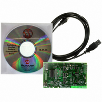
Manufacturer Part Number
TMPSNS-RTD1
Description
BOARD EVAL PT100 RTD TEMP SENSOR
Manufacturer
Microchip Technology
Datasheets
1.MCP3301-CIMS.pdf
(32 pages)
2.PCM18XR1.pdf
(438 pages)
3.MCP6S22DM-PICTL.pdf
(43 pages)
4.TMPSNS-RTD1.pdf
(26 pages)
Specifications of TMPSNS-RTD1
Sensor Type
Temperature
Interface
USB
Embedded
Yes, MCU, 8-Bit
Utilized Ic / Part
MCP3301, MCP6S26, PIC18F2550
Processor To Be Evaluated
MCP6S26, MCP3301, MCP6024, MCP41010, PIC18F2550, TC1071, MCP6002
Data Bus Width
12 bit
Interface Type
USB
Lead Free Status / RoHS Status
Not applicable / Not applicable
Voltage - Supply
-
Sensitivity
-
Sensing Range
-
Lead Free Status / RoHS Status
Lead free / RoHS Compliant, Not applicable / Not applicable


PIC18F2455/2550/4455/4550
SUBWFB
Syntax:
Operands:
Operation:
Status Affected:
Encoding:
Description:
Words:
Cycles:
Example 1:
Example 2:
Example 3:
DS39632E-page 350
Q Cycle Activity:
Before Instruction
After Instruction
Before Instruction
After Instruction
Before Instruction
After Instruction
Decode
REG
W
C
REG
W
C
Z
N
REG
W
C
REG
W
C
Z
N
REG
W
C
REG
W
C
Z
N
Q1
=
=
=
=
=
=
=
=
=
=
=
=
=
=
=
=
=
=
=
=
=
=
=
=
register ‘f’
(f) – (W) – (C) → dest
Subtract W from f with Borrow
SUBWFB
0 ≤ f ≤ 255
d ∈ [0,1]
a ∈ [0,1]
N, OV, C, DC, Z
Subtract W and the Carry flag (borrow)
from register ‘f’ (2’s complement
method). If ‘d’ is ‘0’, the result is stored
in W. If ‘d’ is ‘1’, the result is stored back
in register ‘f’ (default).
If ‘a’ is ‘0’, the Access Bank is selected.
If ‘a’ is ‘1’, the BSR is used to select the
GPR bank (default).
If ‘a’ is ‘0’ and the extended instruction
set is enabled, this instruction operates
in Indexed Literal Offset Addressing
mode whenever f ≤ 95 (5Fh). See
Section 26.2.3 “Byte-Oriented and
Bit-Oriented Instructions in Indexed
Literal Offset Mode” for details.
1
1
SUBWFB
SUBWFB REG, 0, 0
SUBWFB
Read
0101
Q2
19h
0Dh
1
0Ch
0Dh
1
0
0
1Bh
1Ah
0
1Bh
00h
1
1
0
03h
0Eh
1
F5h
0Eh
0
0
1
f {,d {,a}}
10da
REG, 1, 0
REG, 1, 0
(0001 1001)
(0000 1101)
(0000 1011)
(0000 1101)
; result is positive
(0001 1011)
(0001 1010)
(0001 1011)
; result is zero
(0000 0011)
(0000 1101)
(1111 0100)
; [2’s comp]
(0000 1101)
; result is negative
Process
Data
Q3
ffff
destination
Write to
Q4
ffff
SWAPF
Syntax:
Operands:
Operation:
Status Affected:
Encoding:
Description:
Words:
Cycles:
Example:
Q Cycle Activity:
Before Instruction
After Instruction
Decode
REG
REG
Q1
=
=
register ‘f’
Swap f
SWAPF f {,d {,a}}
0 ≤ f ≤ 255
d ∈ [0,1]
a ∈ [0,1]
(f<3:0>) → dest<7:4>,
(f<7:4>) → dest<3:0>
None
The upper and lower nibbles of register
‘f’ are exchanged. If ‘d’ is ‘0’, the result
is placed in W. If ‘d’ is ‘1’, the result is
placed in register ‘f’ (default).
If ‘a’ is ‘0’, the Access Bank is selected.
If ‘a’ is ‘1’, the BSR is used to select the
GPR bank (default).
If ‘a’ is ‘0’ and the extended instruction
set is enabled, this instruction operates
in Indexed Literal Offset Addressing
mode whenever f ≤ 95 (5Fh). See
Section 26.2.3 “Byte-Oriented and
Bit-Oriented Instructions in Indexed
Literal Offset Mode” for details.
1
1
SWAPF
Read
0011
Q2
53h
35h
© 2009 Microchip Technology Inc.
REG, 1, 0
10da
Process
Data
Q3
ffff
destination
Write to
Q4
ffff
Related parts for TMPSNS-RTD1
Image
Part Number
Description
Manufacturer
Datasheet
Request
R

Part Number:
Description:
Manufacturer:
Microchip Technology Inc.
Datasheet:
Part Number:
Description:
Manufacturer:
Microchip Technology Inc.
Datasheet:
Part Number:
Description:
Manufacturer:
Microchip Technology Inc.
Datasheet:
Part Number:
Description:
Manufacturer:
Microchip Technology Inc.
Datasheet:
Part Number:
Description:
Manufacturer:
Microchip Technology Inc.
Datasheet:
Part Number:
Description:
Manufacturer:
Microchip Technology Inc.
Datasheet:
Part Number:
Description:
Manufacturer:
Microchip Technology Inc.
Datasheet:
Part Number:
Description:
Manufacturer:
Microchip Technology Inc.
Datasheet: