C8051F330DK Silicon Laboratories Inc, C8051F330DK Datasheet - Page 3
C8051F330DK
Manufacturer Part Number
C8051F330DK
Description
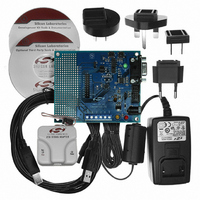
DEV KIT FOR C8051F330/F331
Manufacturer
Silicon Laboratories Inc
Type
MCUr
Specifications of C8051F330DK
Contents
Evaluation Board, Power Supply, USB Cables, Adapter and Documentation
Processor To Be Evaluated
C8051F33x
Interface Type
RS-232
Operating Supply Voltage
7 V to 15 V
Silicon Manufacturer
Silicon Labs
Core Architecture
8051
Silicon Core Number
C8051F330
Silicon Family Name
C8051F33x
Lead Free Status / RoHS Status
Contains lead / RoHS non-compliant
For Use With/related Products
Silicon Laboratories C8051F330, C8051F331
Lead Free Status / Rohs Status
Lead free / RoHS Compliant
Other names
336-1264


Table of Contents
1. System Overview.................................................................................................... 17
2. Absolute Maximum Ratings .................................................................................. 31
3. Global Electrical Characteristics .......................................................................... 32
4. Pinout and Package Definitions............................................................................ 35
5. 10-Bit ADC (ADC0, C8051F330/2/4 only) .............................................................. 41
6. 10-Bit Current Mode DAC (IDA0, C8051F330 only).............................................. 57
7. Voltage Reference (C8051F330/2/4 only).............................................................. 61
8. Comparator0 ........................................................................................................... 65
9. CIP-51 Microcontroller ........................................................................................... 71
1.1. CIP-51™ Microcontroller Core.......................................................................... 22
1.2. On-Chip Memory............................................................................................... 24
1.3. On-Chip Debug Circuitry................................................................................... 25
1.4. Programmable Digital I/O and Crossbar ........................................................... 26
1.5. Serial Ports ....................................................................................................... 26
1.6. Programmable Counter Array ........................................................................... 27
1.7. 10-Bit Analog to Digital Converter..................................................................... 28
1.8. Comparators ..................................................................................................... 29
1.9. 10-bit Current Output DAC................................................................................ 30
5.1. Analog Multiplexer ............................................................................................ 41
5.2. Temperature Sensor ......................................................................................... 42
5.3. Modes of Operation .......................................................................................... 43
5.4. Programmable Window Detector ...................................................................... 51
6.1. IDA0 Output Scheduling ................................................................................... 57
6.2. IDAC Output Mapping....................................................................................... 58
9.1. Instruction Set ................................................................................................... 72
9.2. Memory Organization........................................................................................ 76
1.1.1. Fully 8051 Compatible.............................................................................. 22
1.1.2. Improved Throughput ............................................................................... 22
1.1.3. Additional Features .................................................................................. 23
5.3.1. Starting a Conversion............................................................................... 44
5.3.2. Tracking Modes........................................................................................ 45
5.3.3. Settling Time Requirements ..................................................................... 46
5.4.1. Window Detector In Single-Ended Mode ................................................. 53
5.4.2. Window Detector In Differential Mode...................................................... 54
6.1.1. Update Output On-Demand ..................................................................... 57
6.1.2. Update Output Based on Timer Overflow ................................................ 58
6.1.3. Update Output Based on CNVSTR Edge................................................. 58
9.1.1. Instruction and CPU Timing ..................................................................... 72
9.1.2. MOVX Instruction and Program Memory ................................................. 72
9.2.1. Program Memory...................................................................................... 77
9.2.2. Data Memory............................................................................................ 78
9.2.3. General Purpose Registers ...................................................................... 78
9.2.4. Bit Addressable Locations........................................................................ 78
Rev. 1.7
C8051F330/1/2/3/4/5
3
Related parts for C8051F330DK
Image
Part Number
Description
Manufacturer
Datasheet
Request
R

Part Number:
Description:
SMD/C°/SINGLE-ENDED OUTPUT SILICON OSCILLATOR
Manufacturer:
Silicon Laboratories Inc
Part Number:
Description:
Manufacturer:
Silicon Laboratories Inc
Datasheet:
Part Number:
Description:
N/A N/A/SI4010 AES KEYFOB DEMO WITH LCD RX
Manufacturer:
Silicon Laboratories Inc
Datasheet:
Part Number:
Description:
N/A N/A/SI4010 SIMPLIFIED KEY FOB DEMO WITH LED RX
Manufacturer:
Silicon Laboratories Inc
Datasheet:
Part Number:
Description:
N/A/-40 TO 85 OC/EZLINK MODULE; F930/4432 HIGH BAND (REV E/B1)
Manufacturer:
Silicon Laboratories Inc
Part Number:
Description:
EZLink Module; F930/4432 Low Band (rev e/B1)
Manufacturer:
Silicon Laboratories Inc
Part Number:
Description:
I°/4460 10 DBM RADIO TEST CARD 434 MHZ
Manufacturer:
Silicon Laboratories Inc
Part Number:
Description:
I°/4461 14 DBM RADIO TEST CARD 868 MHZ
Manufacturer:
Silicon Laboratories Inc
Part Number:
Description:
I°/4463 20 DBM RFSWITCH RADIO TEST CARD 460 MHZ
Manufacturer:
Silicon Laboratories Inc
Part Number:
Description:
I°/4463 20 DBM RADIO TEST CARD 868 MHZ
Manufacturer:
Silicon Laboratories Inc
Part Number:
Description:
I°/4463 27 DBM RADIO TEST CARD 868 MHZ
Manufacturer:
Silicon Laboratories Inc
Part Number:
Description:
I°/4463 SKYWORKS 30 DBM RADIO TEST CARD 915 MHZ
Manufacturer:
Silicon Laboratories Inc
Part Number:
Description:
N/A N/A/-40 TO 85 OC/4463 RFMD 30 DBM RADIO TEST CARD 915 MHZ
Manufacturer:
Silicon Laboratories Inc
Part Number:
Description:
I°/4463 20 DBM RADIO TEST CARD 169 MHZ
Manufacturer:
Silicon Laboratories Inc