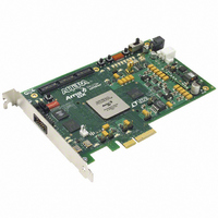
DK-DEV-1AGX60N Altera, DK-DEV-1AGX60N Datasheet - Page 109

DK-DEV-1AGX60N
Manufacturer Part Number
DK-DEV-1AGX60N
Description
KIT DEV ARRIA GX 1AGX60N
Manufacturer
Altera
Series
Arria GXr
Type
FPGAr
Datasheet
1.EP1AGX20CF484C6N.pdf
(234 pages)
Specifications of DK-DEV-1AGX60N
Contents
Dev. Board, Quartus® II Web Edition, Reference Designs, Labs, and Complete Documentation
For Use With/related Products
1AGX60N
Lead Free Status / RoHS Status
Lead free / RoHS Compliant
Other names
544-2372
Available stocks
Company
Part Number
Manufacturer
Quantity
Price
- Current page: 109 of 234
- Download datasheet (4Mb)
Chapter 2: Arria GX Architecture
High-Speed Differential I/O with DPA Support
Figure 2–80. GX Receiver Channel
© December 2009 Altera Corporation
Up to 840 Mbps
f
Eight Phase Clocks
Figure 2–80
An external pin or global or regional clock can drive the fast PLLs, which can output
up to three clocks: two multiplied high-speed clocks to drive the SERDES block
and/or external pin, and a low-speed clock to drive the logic array. In addition, eight
phase-shifted clocks from the V
For more information about fast PLL, refer to the
The eight phase-shifted clocks from the fast PLL feed to the DPA block. The DPA
block selects the closest phase to the center of the serial data eye to sample the
incoming data. This allows the source-synchronous circuitry to capture incoming data
correctly regardless of channel-to-channel or clock-to-channel skew. The DPA block
locks to a phase closest to the serial data phase. The phase-aligned DPA clock is used
to write the data into the synchronizer.
The synchronizer sits between the DPA block and the data realignment and SERDES
circuitry. Because every channel using the DPA block can have a different phase
selected to sample the data, the synchronizer is needed to synchronize the data to the
high-speed clock domain of the data realignment and the SERDES circuitry.
For high-speed source-synchronous interfaces such as POS-PHY 4 and the Parallel
RapidIO standard, the source synchronous clock rate is not a byte- or SERDES-rate
multiple of the data rate. Byte alignment is necessary for these protocols because the
source synchronous clock does not provide a byte or word boundary as the clock is
one half the data rate, not one eighth. The Arria GX device’s high-speed differential
I/O circuitry provides dedicated data realignment circuitry for user-controlled byte
boundary shifting. This simplifies designs while saving ALM resources. You can use
an ALM-based state machine to signal the shift of receiver byte boundaries until a
specified pattern is detected to indicate byte alignment.
+
–
refclk
data
Fast
PLL
8
retimed_data
DPA
shows the block diagram of the Arria GX receiver channel.
DPA_clk
Synchronizer
diffioclk
load_en
D
Q
CO
can feed to the DPA circuitry.
Data Realignment
Circuitry
Dedicated
Interface
Receiver
PLLs in Arria GX Devices
Arria GX Device Handbook, Volume 1
Data to R4, R24, C4, or
direct link interconnect
Regional or
global clock
10
chapter.
2–103
Related parts for DK-DEV-1AGX60N
Image
Part Number
Description
Manufacturer
Datasheet
Request
R

Part Number:
Description:
KIT DEV ARRIA II GX FPGA 2AGX125
Manufacturer:
Altera
Datasheet:

Part Number:
Description:
KIT DEV CYCLONE III LS EP3CLS200
Manufacturer:
Altera
Datasheet:

Part Number:
Description:
KIT DEV STRATIX IV FPGA 4SE530
Manufacturer:
Altera
Datasheet:

Part Number:
Description:
KIT DEV FPGA 2AGX260 W/6.375G TX
Manufacturer:
Altera
Datasheet:

Part Number:
Description:
KIT DEV MAX V 5M570Z
Manufacturer:
Altera
Datasheet:

Part Number:
Description:
KIT DEV STRATIX V FPGA 5SGXEA7
Manufacturer:
Altera
Datasheet:

Part Number:
Description:
KIT DEVELOPMENT STRATIX III
Manufacturer:
Altera
Datasheet:

Part Number:
Description:
KIT DEVELOPMENT STRATIX IV
Manufacturer:
Altera
Datasheet:

Part Number:
Description:
KIT STARTER CYCLONE IV GX
Manufacturer:
Altera
Datasheet:

Part Number:
Description:
KIT DEVELOPMENT STRATIX IV
Manufacturer:
Altera
Datasheet:

Part Number:
Description:
CPLD, EP610 Family, ECMOS Process, 300 Gates, 16 Macro Cells, 16 Reg., 16 User I/Os, 5V Supply, 35 Speed Grade, 24DIP
Manufacturer:
Altera Corporation
Datasheet:

Part Number:
Description:
CPLD, EP610 Family, ECMOS Process, 300 Gates, 16 Macro Cells, 16 Reg., 16 User I/Os, 5V Supply, 15 Speed Grade, 24DIP
Manufacturer:
Altera Corporation
Datasheet:


