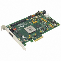
DK-DEV-1AGX60N Altera, DK-DEV-1AGX60N Datasheet - Page 70

DK-DEV-1AGX60N
Manufacturer Part Number
DK-DEV-1AGX60N
Description
KIT DEV ARRIA GX 1AGX60N
Manufacturer
Altera
Series
Arria GXr
Type
FPGAr
Datasheet
1.EP1AGX20CF484C6N.pdf
(234 pages)
Specifications of DK-DEV-1AGX60N
Contents
Dev. Board, Quartus® II Web Edition, Reference Designs, Labs, and Complete Documentation
For Use With/related Products
1AGX60N
Lead Free Status / RoHS Status
Lead free / RoHS Compliant
Other names
544-2372
Available stocks
Company
Part Number
Manufacturer
Quantity
Price
- Current page: 70 of 234
- Download datasheet (4Mb)
2–64
Figure 2–53. DSP Block Interface to Interconnect
Arria GX Device Handbook, Volume 1
f
C4 Interconnect
LAB
A bus of 44 control signals feeds the entire DSP block. These signals include clocks,
asynchronous clears, clock enables, signed and unsigned control signals, addition and
subtraction control signals, rounding and saturation control signals, and accumulator
synchronous loads. The clock signals are routed from LAB row clocks and are
generated from specific LAB rows at the DSP block interface. The LAB row source for
control signals, data inputs, and outputs is shown in
For more information about DSP blocks, refer to the
chapter.
18
DSP Block to
LAB Row Interface
Block Interconnect Region
Direct Link Interconnect
from Adjacent LAB
36
16
Row Interface
36
12
Block
36 Inputs per Row
R4 Interconnect
16
Control
A[17..0]
B[17..0]
DSP Block
Row Structure
OA[17..0]
OB[17..0]
36 Outputs per Row
Direct Link Outputs
to Adjacent LABs
36
DSP Blocks in Arria GX Devices
36
Table
© December 2009 Altera Corporation
2–15.
Chapter 2: Arria GX Architecture
Direct Link Interconnect
from Adjacent LAB
Digital Signal Processing Block
LAB
Related parts for DK-DEV-1AGX60N
Image
Part Number
Description
Manufacturer
Datasheet
Request
R

Part Number:
Description:
KIT DEV ARRIA II GX FPGA 2AGX125
Manufacturer:
Altera
Datasheet:

Part Number:
Description:
KIT DEV CYCLONE III LS EP3CLS200
Manufacturer:
Altera
Datasheet:

Part Number:
Description:
KIT DEV STRATIX IV FPGA 4SE530
Manufacturer:
Altera
Datasheet:

Part Number:
Description:
KIT DEV FPGA 2AGX260 W/6.375G TX
Manufacturer:
Altera
Datasheet:

Part Number:
Description:
KIT DEV MAX V 5M570Z
Manufacturer:
Altera
Datasheet:

Part Number:
Description:
KIT DEV STRATIX V FPGA 5SGXEA7
Manufacturer:
Altera
Datasheet:

Part Number:
Description:
KIT DEVELOPMENT STRATIX III
Manufacturer:
Altera
Datasheet:

Part Number:
Description:
KIT DEVELOPMENT STRATIX IV
Manufacturer:
Altera
Datasheet:

Part Number:
Description:
KIT STARTER CYCLONE IV GX
Manufacturer:
Altera
Datasheet:

Part Number:
Description:
KIT DEVELOPMENT STRATIX IV
Manufacturer:
Altera
Datasheet:

Part Number:
Description:
CPLD, EP610 Family, ECMOS Process, 300 Gates, 16 Macro Cells, 16 Reg., 16 User I/Os, 5V Supply, 35 Speed Grade, 24DIP
Manufacturer:
Altera Corporation
Datasheet:

Part Number:
Description:
CPLD, EP610 Family, ECMOS Process, 300 Gates, 16 Macro Cells, 16 Reg., 16 User I/Os, 5V Supply, 15 Speed Grade, 24DIP
Manufacturer:
Altera Corporation
Datasheet:


